Thank you for visiting nature.com. You are using a browser version with limited support for CSS. To obtain the best experience, we recommend you use a more up to date browser (or turn off compatibility mode in Internet Explorer). In the meantime, to ensure continued support, we are displaying the site without styles and JavaScript.
- View all journals
- My Account Login
- Explore content
- About the journal
- Publish with us
- Sign up for alerts
- Review Article
- Open access
- Published: 19 December 2023

Advances in high-performance MEMS pressure sensors: design, fabrication, and packaging
- Xiangguang Han 1 , 2 , 3 ,
- Mimi Huang 1 , 2 , 3 ,
- Zutang Wu 4 ,
- Yi Gao 1 , 2 , 3 ,
- Yong Xia 1 , 2 , 3 ,
- Ping Yang 1 , 2 , 3 ,
- Shu Fan 1 , 2 , 3 ,
- Xuhao Lu 1 , 2 , 3 ,
- Xiaokai Yang 1 , 2 , 3 ,
- Lin Liang 1 , 2 , 3 ,
- Wenbi Su 1 , 2 , 3 ,
- Lu Wang 1 , 2 , 3 ,
- Zeyu Cui 1 , 2 , 3 ,
- Yihe Zhao 1 , 2 , 3 ,
- Zhikang Li ORCID: orcid.org/0000-0001-7017-0097 1 , 2 , 3 ,
- Libo Zhao ORCID: orcid.org/0000-0001-6101-8173 1 , 2 , 3 &
- Zhuangde Jiang 1 , 2 , 3
Microsystems & Nanoengineering volume 9 , Article number: 156 ( 2023 ) Cite this article
5850 Accesses
6 Altmetric
Metrics details
- Electrical and electronic engineering
- Electronic properties and materials
Pressure sensors play a vital role in aerospace, automotive, medical, and consumer electronics. Although microelectromechanical system (MEMS)-based pressure sensors have been widely used for decades, new trends in pressure sensors, including higher sensitivity, higher accuracy, better multifunctionality, smaller chip size, and smaller package size, have recently emerged. The demand for performance upgradation has led to breakthroughs in sensor materials, design, fabrication, and packaging methods, which have emerged frequently in recent decades. This paper reviews common new trends in MEMS pressure sensors, including minute differential pressure sensors (MDPSs), resonant pressure sensors (RPSs), integrated pressure sensors, miniaturized pressure chips, and leadless pressure sensors. To realize an extremely sensitive MDPS with broad application potential, including in medical ventilators and fire residual pressure monitors, the “beam-membrane-island” sensor design exhibits the best performance of 66 μV/V/kPa with a natural frequency of 11.3 kHz. In high-accuracy applications, silicon and quartz RPS are analyzed, and both materials show ±0.01%FS accuracy with respect to varying temperature coefficient of frequency ( TCF ) control methods. To improve MEMS sensor integration, different integrated “pressure + x ” sensor designs and fabrication methods are compared. In this realm, the intercoupling effect still requires further investigation. Typical fabrication methods for microsized pressure sensor chips are also reviewed. To date, the chip thickness size can be controlled to be <0.1 mm, which is advantageous for implant sensors. Furthermore, a leadless pressure sensor was analyzed, offering an extremely small package size and harsh environmental compatibility. This review is structured as follows. The background of pressure sensors is first presented. Then, an in-depth introduction to MEMS pressure sensors based on different application scenarios is provided. Additionally, their respective characteristics and significant advancements are analyzed and summarized. Finally, development trends of MEMS pressure sensors in different fields are analyzed.
Novel resonant pressure sensor based on piezoresistive detection and symmetrical in-plane mode vibration
Xiangguang Han, Qi Mao, … Zhuangde Jiang

Switch mode capacitive pressure sensors
Nabil Shalabi, Kyle Searles & Kenichi Takahata

A resonant high-pressure microsensor based on a composite pressure-sensitive mechanism of diaphragm bending and volume compression
Pan Qian, Zongze Yu, … Junbo Wang
Introduction
Pressure is a fundamental parameter for measuring internal fluid pressure and is crucial for fluid control and equipment status monitoring. Pressure sensors thus find extensive applications in industries such as automotive, medical, and aerospace. Through precise pressure measurements, equipment conditions can be accurately monitored, and potential failures can be predicted. Furthermore, with the ongoing advancement in smart instruments over the past few decades, there has been a demand for pressure sensors to satisfy stricter technical requirements. These include higher precision, enhanced environmental adaptability, finer resolution, and smaller chip/package sizes 1 , 2 , 3 , 4 .
Pressure sensors can be categorized based on their sensing mechanisms into piezoresistive, capacitive, resonant, piezoelectric sensors, and more 5 , 6 , 7 , 8 . The piezoresistive effect, which was discovered by Smith in 1954 9 , has led to the widespread use of piezoresistive sensors 10 , 11 . These sensors primarily measure pressure using a Wheatstone bridge. A pivotal step in chip fabrication that has catalyzed the mass production of piezoresistive pressure sensors (PPS) is diaphragm etching 12 , 13 . This process is bifurcated into wet and dry etching. Wet etching is further differentiated into anisotropic and isotropic methods. The deep reactive ion etching (DRIE) method, which was introduced in 1993 14 , minimizes lateral etching by alternating between passivation and etching phases 15 . This innovation led to a marked reduction in chip size and cost. However, piezoresistive sensors exhibit a high temperature coefficient of zero point ( TCZ ) and a high temperature coefficient of sensitivity ( TCS ) 16 , diminishing their accuracy across extensive temperature ranges 17 , 18 . Bao demonstrated that the TCS can be offset by balancing the temperature coefficient of resistance ( TCR ) and temperature coefficient of piezoresistivity ( TCP ) 19 . Factors such as piezoresistor TCR , fabrication discrepancies, and package stress add complexity to realizing high-precision pressure measurements 20 . Currently, only a handful of companies have successfully commercialized high-precision single-crystal silicon (SCS) pressure sensors. Thus, high-performance PPS still needs further research.
In addition to SCS pressure sensors, a polycrystalline silicon pressure sensor (PSPS) was proposed by French and Evans in 1985 21 . This sensor was used to comprehensively examine the piezoresistive effect between monocrystalline silicon and the barrier region. To describe the theoretical model of the sensitivity coefficient of polycrystalline silicon pressure sensors more accurately under different doping concentrations, Chuai et al. established a tunnel piezoresistive theory in 2012 22 . Currently, PSPS is seldom mass-produced, and its accuracy needs to be further improved 23 , 24 . As another important piezoresistive pressure sensor, thin-film pressure sensors are based on the strain effect of metals and are widely used in the automotive electronics and aerospace fields, especially as ultralow-temperature pressure sensors. However, the fabrication cost is excessively high for batch consumer electronic applications. The sensing material system also requires further expansion because the sensing unit is mainly concentrated in Ni/Cr material systems 25 , 26 , 27 , 28 with a limited gauge factor.
In addition to PPS, capacitive pressure sensors (CPS) measure pressure chiefly by monitoring the capacitance change between their sensing plates. Notably, CPSs consume significantly less power when compared to piezoresistive or resonant pressure sensors (RPSs) 29 , making them popular choices for consumer electronics and industrial applications. An advantage of CPSs is their improved temperature stability, as their capacitance is less affected by temperature 30 . However, CPSs are more susceptible to variations in media dielectric properties, such as the parasitic capacitance from measurement circuits or the pressure media 31 , 32 , 33 . This limitation can negatively impact their precision. Consequently, only a few CPSs have reported precision values exceeding 0.05%FS. Moreover, some RPSs operate by recording the change in a resonant beam’s stress state due to pressure. This pressure change results in a linear shift of the beam’s natural frequency. Due to their high gauge factor, high-quality factor, and reliance on the elastic modulus to determine output frequency, RPSs offer exceptional detection resolution and accuracy, making them ideal for metrological sensors. However, their intricate structure and fabrication process increase their cost. Moreover, their response frequency is limited by factors such as phase-locked loops and packaging techniques, rendering them less suitable for high-response pressure detection 7 , 8 , 20 .
Microelectromechanical system (MEMS) pressure sensors offer several advantages, including ease of batch production, miniaturization, cost-effectiveness, and the capability to readily fabricate complex structures. Therefore, they occupy an increasingly larger share of the pressure sensor market. Over the past two decades, advancements in MEMS sensor technology, encompassing principles, theory, design, and fabrication techniques (such as bulk silicon etching, thin-film fabrication, and low-temperature bonding), have facilitated the rapid advancement and diversification of pressure sensors for various applications. Newer pressure-sensing elements leveraging innovative technologies and packaging methods offer enhanced measurement accuracy, size, and broader temperature adaptability 34 , 35 . Furthermore, the integration of emerging materials, such as third-generation semiconductor materials, graphene, and nanowires, in pressure sensors has significantly elevated their performance 36 , 37 .
Relevant MEMS pressure sensor trends include drives for higher sensitivity, higher accuracy, multiparameter integration, smaller chip size, smaller package size, and harsh environment-compatible devices. This paper reviews the corresponding sensors in various applications, including minute differential pressure sensors (MDPSs), RPSs, integrated pressure sensors, miniaturized pressure sensors, and leadless packaged pressure sensors. The working principles, research progress, technical difficulties, and prospects are discussed separately.
Minute differential pressure sensors
MDPSs have found applications in diverse fields, including biomedicine 38 , 39 , aerospace 40 , blast damage assessment 41 , and air pressure monitoring in fire exits 42 , 43 , underscoring their significant engineering and medical value. An MDPS generally refers to a pressure sensor capable of measuring pressure ranges below 10 kPa. This indicates that the differential pressure across the diaphragm is usually minimal. As medical equipment evolves, there is a growing demand for MDPSs with superior measurement resolution, enhanced frequency response, reduced size, and cost-effectiveness. Designing and fabricating MDPSs present greater challenges when compared to other piezoresistive sensors, especially in ensuring high sensitivity and embedding a stable piezoresistor on an ultrathin, low-residual-stress pressure diaphragm. Therefore, over the past 20 years, many researchers have conducted in-depth studies on MDPSs based on their principles, materials, and structures.
MDPSs typically measure pressure ranges spanning just a few kPa or even down to hundreds of Pa. Consequently, they demand high sensitivity and resolution, leading to sensing diaphragms that often possess a high width-to-thickness ratio. For capacitive MDPSs, their large outer diameter and pronounced nonlinearity limit their application in minute pressure sensing 44 , 45 . However, piezoresistive pressure sensors exhibit favorable linearity and capitalize on the stress concentration effect of the sensing unit. This feature makes them conducive to chip miniaturization, explaining their extensive investigation in the literature 46 . To satisfy the sensitivity requirements of MDPSs, researchers introduced a variety of sensitive structures for ultrasensitive MEMS sensors. Over time, MDPSs have evolved from “C”-type membranes 5 (flat membranes) to “E”-type membranes 47 (island membranes) and then to “beam–membrane–island” configurations 48 , 49 , witnessing progressive enhancements in sensitivity.
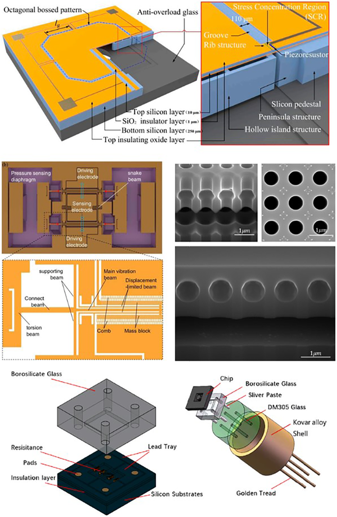
To improve the sensitivity of MDPSs, a sensitive resistor is set in the stress concentration area to eliminate unnecessary energy loss. Yu et al. 47 combined a surface cross-beam and backside islands based on a C-type membrane structure (Fig. 1a ). The design combination further localizes the stress concentration on the beams near the diaphragm edge, as illustrated in Fig. 1b . This design results in a sensitivity output that surpasses both the C-type and E-type structures, as depicted in Fig. 1c . Additionally, with the inclusion of the rectangular silicon island limiter, the diaphragm can endure atmospheric pressures up to 200 times its pressure range. The results show that the structure can significantly improve the sensitivity and reach 11.098 μV/V/Pa in the pressure range of 0–500 Pa. However, the nonlinearity is only 3.046%FS.

a MDPS characterized by a “beam-membrane-quad-island” (BMQI) structure (front and bottom view of the chip) 47 . b Stress distribution and stress path of the structure. c Comparison of the von Mises stresses of the three structure types. d Four-beam-bossed-membrane (FBBM) structure (front and back review) 50 . e Back review of FBBM 50 . f Stress distribution curve of the path 50 . g Backside view of an ultrahigh-sensitivity pressure sensor chip 51 . h Circuit on the CBM sensor. i Structure of CBM and X-direction stress distribution curve 52
Li et al. 50 enhanced the stress concentration effect using a crossbeam film and introduced a high-sensitivity structure by integrating the film with an annular groove, as illustrated in Fig. 1d, e . In this configuration, the crossbeam serves as a supporting rib, preventing undue deformation. Four grooves are etched adjacent to the membrane, inducing a rapid change in the lateral stiffness of the sensing area and amplifying the stress concentration to 40 MPa, as demonstrated in Fig. 1f . This design exhibits a sensitivity of 30.9 mV/V/kPa within a pressure range of 145 Pa and maintains a nonlinearity of just 0.25% FS. However, the design presents a sizable chip dimension of 7 mm × 7 mm. Basov et al. 51 , in their pursuit of heightened sensitivity, created MDPS islands using wet etching, incorporating a “multi-island” design for stress concentration, as depicted in Fig. 1g . The concentration is determined by the spacing between the islands. After optimization, the sensitivity reached an impressive 34.5 mV/V/kPa, with nonlinearity surpassing 0.81% FS within a 500 Pa pressure scope. However, the chip measures 6.15 mm × 6.15 mm. Tian et al. 52 introduced a cross-beam membrane (CBM), showcased in Fig. 1h , which boasts superior stress concentration capabilities. It delivers an accuracy of ~0.24%FS within a 10 kPa pressure range, with a chip size of 4.3 mm × 4.3 mm.
To satisfy the requirements for monitoring infant respiratory pressure and pipette height, there is a compelling need to boost sensor sensitivity. Xu advanced the “beam–island–membrane” structure by incorporating the “peninsula island” design, which amplified the stress concentration effect 48 , 49 , 53 , as illustrated in Fig. 3a, b . Additionally, shallow grooves were etched at the forefront of the pressure-bearing diaphragm. The ridges that form between these grooves cause a pronounced shift in lateral stiffness, preventing strain energy dispersion and amassing stress >50 MPa, as depicted in Fig. 3c . The innovative hollow island design curtails excessive diaphragm mass, enhancing the sensor’s dynamic performance. This configuration yields an impressive sensitivity of 66 μV/V/kPa and maintains a nonlinearity of 0.33%FS within a 500 Pa range.
Different MDPS pressure sensors adopt similar fabrication processes, including sensitive piezoresistor doping and wet/dry etching, as shown in Fig. 2 . In most designs, an etching-stop layer is introduced for thickness control, which is difficult to realize using single-crystal silicon direct etching. Given that the diaphragm is too thin to be sensitive to its stress state, there is a lack of stress control methods. Thus, it should be investigated in the future.

a Process flow, a-1 Cleaning SOI wafer, a-2 Boron implantation to form heavily doped section, a-3 Boron implantation and thermal annealing to form the piezoresistors, a-4 Contact hole etching, a-5 Front side RIE etching to form grooves, a-6 Back side DRIE etching to from peninsula-island structure, a-7 Bonding glass base, b Top view of the typical MDPS
In addition to driving modified structural design, signal amplification can increase pressure sensitivity and resolution. Basov et al. 54 proposed a piezoresistive differential amplifier using an on-chip negative-feedback loop. The combination design with the on-chip circuit amplifier and stress concentration structure is shown in Fig. 3 d, and a schematic of the electrical circuit is shown in Fig. 3 e. After amplification, the MDPS sensitivity reaches 44.9 mV/V/kPa, and the TCZ is ~0.094% FS/°C with a 550-fold overload ability.

a Peninsula island-based bossed diaphragm structure 48 , 49 , 53 . b Planar construction view of the proposed structure 48 , 49 , 53 . c Stress difference from the central point to the diaphragm edge 48 , 49 , 53 . d Ultrahigh-sensitivity pressure sensor (top view), 185 . e Electrical circuit 185 . f Structural schematic of the improved capacitive resonant MDPS 55 . g Variation in the resonant frequency of the transducer with pressure 55
In addition to piezoresistive sensors, miniature capacitive resonant pressure sensors (RPSs) have been developed with high accuracy and resolution. Li et al. 55 developed a resonant pressure sensor in which the pressure diaphragm stress changes under pressure, causing the stiffness of the diaphragm to shift linearly, and the frequency reflects the pressure, as shown in Fig. 3f . The test results are shown in Fig. 3g . The frequency pressure sensitivity is ~−2.54 ppm/Pa (7.46 Hz/Pa); the nonlinearity is <0.01%FS, which is much better than that of the piezoresistive sensor. However, this capacitive RPS requires more complicated conditioning circuits and relies on the pressure medium density. Thus, its applications are highly limited.
The specifications of the reported MDPSs are listed in Table 1 . The “slot + island + peninsula” structure has higher sensor sensitivity. However, with a large in-plane size of 5 mm × 5 mm, the size of the sensor chip should be further reduced to satisfy the requirements for miniaturized packaging. Moreover, research on MDPSs is currently mainly focused on improving the sensitivity, which nearly satisfies the resolution requirements of common medical equipment. In many applications, such as shockwaves and altimeters in flight control, the dynamic characteristics of the sensor are needed. Thus, a decoupling method for sensitivity and frequency should be investigated. Additionally, the nonlinearity of the reported sensor still requires improvement, and the stress of the multilayer diaphragm at different temperatures should be studied to realize such improvement because the diaphragm is usually thin and sensitive to residual stress. The resonant-capacitance MDPS exhibits better accuracy than other designs. However, it requires a complex control circuit.
High-precision pressure sensors are critically important in sectors such as aerospace, oil exploration, meteorological observation, and national defense. They are often employed to measure fluid pressures in ambient environments, cabin atmospheres, fuselage hydraulic systems, engines, and the gases and liquids of oxygen masks 40 , 56 . Within aviation’s air data detection systems, an integrated data system typically necessitates over ten high-precision pressure sensors. These sensors are expected to achieve accuracy surpassing ±0.05%FS and ensure long-term stability in their performance 57 , 58 , 59 . High-precision pressure sensors play an irreplaceable role in the fields of meteorological measurements and air data systems. The accuracy is generally required to be an order of magnitude higher than that of the currently available sensors, and the basic error is usually expected to be <0.02%FS 10 .
Currently, the global landscape of high-precision pressure sensors predominantly features RPS with an extensive operational temperature range. Moreover, only a few piezoresistive sensors can realize an accuracy of 0.05%FS 60 , 61 , 62 . However, they often exhibit inferior temperature stability. Over recent decades, extensive studies on RPSs have delved into their sensitive materials, structures, packaging solutions, and methods of excitation and detection. This discussion will explore the current research on RPSs, particularly focusing on their excitation and detection methods. The Q -factor is a pivotal metric for RPS, which indicates the resolution ability to detect resonant frequencies. The pressure resolution is essentially contingent upon the Q -factor. Numerous efforts have aimed to elevate the Q -factor by mitigating sources of damping, such as air and thermoelastic damping.
Piezoelectric RPS
Piezoelectric conversion serves dual purposes: it detects mechanical deformation via the piezoelectric effect and excites mechanical structures to induce vibrations via the inverse piezoelectric effect. The latter purpose is particularly employed to stimulate the resonant beam, with the stimulation directed along a specific crystal axis of the piezoelectric material 63 . Most reported piezoelectric resonant devices utilize quartz crystals, renowned for their piezoelectric effects, or thin-layer Al 5 N 3 produced via magnetron sputtering. Alternatives, such as ZnO or PZT, are less congruent with semiconductor technology. Quartz piezoelectric crystal materials, known for their minimal hysteresis, high Q -factor, and commendable temperature stability 64 , have been extensively adopted in crystal oscillators. Thus, they emerge as a prime material choice for RPS fabrication. In quartz RPS designs, the quartz crystal beam concurrently operates as the driver and detector.
Zhao 65 , 66 , 67 introduced a range of differential RPSs utilizing piezoelectric quartz resonant beams. The resonator undergoes fabrication through anisotropic etching, and the quartz sensing component is affixed to a silicon membrane, as depicted in Fig. 4a . Using side-magnetron sputtering, excitation and detection electrodes are produced, as illustrated in Fig. 4b . Testing revealed an accuracy surpassing 0.05% FS within the range of 10 kPa. To mitigate temperature sensitivity, dual differential resonators were integrated to compensate for temperature and stress. Nonetheless, the mismatch in the coefficient of thermal expansion ( CTE ) between the quartz resonator and silicon diaphragm results in significant thermal stress, compromising accuracy. The in-plane dimension of the quartz resonant sensor chip measured ~8 mm, supporting that the size can be further reduced, as indicated in Fig. 4c .

a Stress simulation of differential output tuning fork tines 65 . b Main fabrication process of the DETF quartz resonator 65 . c Photograph of the tuning fork prototype 65 . d Packaged pressure sensor prototype with a tuning fork and stainless-steel package 68 , 69 . e Photograph of the EPSON quartz pressure sensor 69 . f Overall structural diagram of a flexible hinge lever 70 . g Main structural diagram of the sensor 70 . h Photograph of the sensor before packaging 70
To address challenges associated with assembling quartz crystal sensing elements and pressure transfer structures, researchers combined traditional machining with MEMS processes. Specifically, wet etching is used for shaping the quartz structure, while traditional precision machining helps to realize the pressure conversion element. The quartz RPS designed by Ren 68 (depicted in Fig. 4d ) and the Epson Company 69 (illustrated in Fig. 4e ) feature a metal base and tuning fork resonator. They offer a repeatability of 0.005%FS and hysteresis of 0.008%FS. Additionally, Zhang et al. 70 integrated a mechanical lever structure (Fig. 4f ) with three resonators, as represented in Fig. 4g and h . This device realized a high precision of ±0.01% FS over a range of 100 kPa. However, this type of packaging approach demands exact machining and assembly standards. Coupled with the size and intricacy of the package, the resultant costs are elevated. Therefore, further refinements to shrink the design of quartz RPSs are warranted.
Capacitive resonant pressure sensor
In addition to piezoelectric RPSs, breakthroughs in silicon-based RPSs, including capacitive, piezoresistive, and magnetic RPSs, have been realized in recent years. Electrostatic excitation is currently the most widely used excitation method for resonant sensors such as resonant pressure, acceleration, and gyroscopes 71 , 72 , 73 . Electrostatic excitation refers to the use of an electrostatic force between the driving and fixed plates by applying an AC + DC voltage with a driving frequency similar to the resonant frequency. Capacitance detection identifies the resonant frequency point of the resonator by detecting the capacitance changes during vibrations. Capacitance RPS has a simpler fabrication process than piezoelectric, piezoresistive, and other preparation processes, including etching and bonding, and thereby has attracted the attention of many researchers.
Ren et al. proposed an RPS based on a double-ended fixed-branch tuning fork structure 74 , 75 , as shown in Fig. 5a . This design used SOI release technology to realize the suspension of the resonator structure, and a nonmetal pad was introduced because most metals are incompatible with the HF solution, as shown in Fig. 5b . In the no-pad bonding technique, the gold wire bonds directly to the silicon surface, which can easily lead to detachment and compromise the sensor’s reliability. When compared to the fabrication technique that employs wet etching and fusion bonding of silicon islands, this challenge is considerably reduced. Testing indicates a sensitivity of ~10.86 Hz/kPa, with a basic measurement error of ±0.02%FS. Nonetheless, the sensor’s quality factor was low, as the resonator was not vacuum-packaged, as depicted in Fig. 5c . Furthermore, given the minimal Δ C during vibration, Sun 75 introduced a new expanded capacitance driving and detection structure. This structure was realized by altering the interface area relative to the electrode distance, as illustrated in Fig. 5d , which eases signal detection challenges.

a Schematic of RPS proposed by Ren 74 , 75 . b Fabrication process 74 , 75 . c RPS package with transistor outline (TO) base and Kovar Cover 74 , 75 . d New tuning fork structure for the RPS. e Design structure of the balanced double-ended tuning fork (BDETF) resonator 76 , 78 . f Comparison of out-of-plane displacements for different beam structures 76 , 78
For capacitance excitation, it is crucial to maintain a consistent driving force across the full pressure range, particularly for closed-loop control. Recognizing the significant out-of-plane displacement discrepancy between the fixed and movable electrodes of the capacitive detection RPS under stress, Du et al. 76 , 77 , 78 introduced a dual-diaphragm RPS design, depicted in Fig. 5e . This design utilizes a composite beam structure, which considerably reduces the out-of-plane displacement of the resonator’s movable electrode, as illustrated in Fig. 5f . Leveraging the anodic bonding auxiliary getter process, they realized high-vacuum packaging. Consequently, the quality factor surpassed 20,000, with the sensor sensitivity reaching 30 Hz/kPa.
In capacitance-based RPS systems, the change in capacitance Δ C , which is rooted in interdigital capacitance, is typically minuscule—often at the fF scale. Thus, it is challenging to detect and often necessitates a complex CV conversion circuit with expansive gain and frequency response. Furthermore, significant crosstalk can arise between the excitation and detection electrodes, leading to pronounced interference in closed-loop control. To address this issue, Du 76 implemented a single pickup electrode situated between the two resonating beams. With this arrangement, during symmetrical resonator vibration, the capacitor functions as expected. Conversely, when there is a unilateral resonator vibration, the capacitance variations from the two pickup electrodes neutralize each other. This design essentially shields the same-side vibration mode.
Electromagnetic RPS
An RPS utilizing electromagnetic excitation/detection mainly leverages the alternating Lorentz force. This force is produced by the alternating current acting on a resonant beam within a constant magnetic field, prompting the resonant beam to oscillate. When the resonator achieves a state of resonance, the oscillating detection beam intersects the magnetic field lines, and the resulting electromagnetic induction generates a signal that marks the resonance frequency point. Unlike the previously discussed resonant sensors, an electromagnetic device does not require intricate excitation or pickup structures. It simply demands an alternating current to be channeled through the driving beam and AC signal detection on the detecting beam. This simplicity in design and manufacturing has catalyzed further research and successful commercialization 79 , 80 .
Wang et al. 81 , 82 , 83 pioneered various RPSs utilizing electromagnetic techniques. To enhance the sensor’s temperature stability, they employed a differential frequency output method, as depicted in Fig. 6b . This method incorporates two or three resonators to decouple the pressure and temperature signals, subsequently reducing the TCF , as illustrated in Fig. 6c . The resonator comprises “H”-type resonant beams with a single-sided vibration mode chosen as the operational mode, as shown in Fig. 6a . To guarantee a high-quality factor, they leveraged anodic bonding technology and a getter process to ensure vacuum packaging. In addition to the differential approach, a unique stress-isolation structure was introduced to counteract the package stress, thereby further minimizing the TCF . Within a pressure range of 100 kPa, the sensor showed a sensitivity of 89.86 Hz/kPa, resolution of 10 Pa, and nonlinearity of <0.01% FS. Additionally, for high-precision MDPS applications, they integrated the “island–diaphragm–beam” design to enhance RPS sensitivity, as evident in Fig. 6d . Their findings demonstrated accuracy surpassing 0.05%FS in a 1-kPa application, as highlighted in Fig. 6e .

a Resonator based on electromagnetic excitation and detection, where the first resonant mode is adopted as the working mode 81 , 82 . b Schematic of the differential pressure sensor with double “H”-type double-clamped resonant beams 81 , 82 . c Comparison of errors before and after differential compensation 81 , 82 . d Schematic of the developed micromachined resonant low-pressure sensor. e Intrinsic frequency shifts of the central (blue) and side (red) beams and differential outputs (green) as functions of low pressure at room temperature. f Front/back views of the microsensor chip, side view of the microsensor chip and layer-by-layer view of the core pressure-sensitive element with a stress isolation layer. g Differential RPS developed by Yokawaga 84 , 85 , 86 . h Cross-sectional view of the differential RPS chip
High-precision differential pressure RPSs are rarely explored and documented, primarily due to the challenges of negating and compensating for the static pressure on either side of the diaphragm and temperature variations. To address this challenge, Wang 83 , 84 introduced a differential RPS incorporating a petite electromagnetic resonator and multilayer-assembled diaphragm, as depicted in Fig. 6f . Similarly, Yokogawa presented a differential RPS tailored for industrial usage based on electromagnetic excitation/detection. This innovation has since been successfully commercialized 85 , 86 , 87 , 88 , 89 and is illustrated in Fig. 6g . Their design integrates two sets of “H”-shaped resonant beams. Unlike Wang et al.’s research, they opted for an out-of-plane vibration mode, resulting in a reduced resonant layer thickness. To amplify sensitivity, the resonators were strategically positioned at both the diaphragm’s center and periphery, inducing tension and compression, respectively. This layout, visualized in Fig. 6h , adeptly minimized TCF . The ’fabrication of the resonator leveraged epitaxial and anisotropic etching techniques, resulting in a Q -factor exceeding 50,000, a TCF under 40 ppm/°C, a fundamental error less than ±0.02%FS, and a stability of ±0.1%FS over a decade. Moreover, given that both sides of the diaphragm are exposed to pressure media, the sensor can be used for gauge pressure or differential pressure measurements, making it one of the few reported gauge RPSs.
Piezoresistive detection RPS
The excitation method for piezoresistive detection is driven by an electrostatic force, which is the same as that for the capacitance detection of RPS. Piezoresistive pick-up resistors are typically arranged in the stress concentration area of the resonant beam, and the resonant frequency is detected by monitoring the change in resistance. Compared to the capacitive detection method, piezoresistive detection has a larger output signal and simpler vibration pickup structure. However, because the piezoresistor fabrication process is more complex than that of the capacitive interdigitated electrode, there is a lack of studies focusing on the piezoresistive detection of RPS 90 , 91 .
In 2009, Druck Co. developed a commercialized RPS based on electrostatic excitation/piezoresistive detection and proposed an electrical connection for the resonator 59 , 92 (Fig. 7a, and b ). The sensor comprised four layers: a vacuum packaging layer, resonant layer, sensitive film layer, and base glass layer (shown in Fig. 7c ). The sensor was mainly prepared via deep reactive ion etching (DRIE) and silicon–silicon bonding, and its Q -factor was >30,000. The accuracy is better than 0.01%FS, and the annual stability is better than ±0.01%, setting it as the benchmark product in the high-accuracy RPS industry.

a 3D schematic of the main components of lateral RPS 91 , 92 . b Schematic of electrical connections to the resonator 59 , 91 , 92 . c Cross-sectional view of the Druck RPS chip 59 , 91 , 92 . d Schematic of microfabricated differential piezoresistive detection of RPS 93 . e Setup and working mode simulation of double-ended tuning forks relying on comb-drive actuation and piezoresistive detection 93 . f Schematic of a resonator with a coupling-beam-enhanced DETF 94 , 96 . g Vacuum package schematic of anodic bonding 94 , 96 . h TCF self-compensated method with stress and TCE contraction 94 , 96
Yan et al. 93 also developed a differential RPS based on the piezoresistive detection method, which shielded the signal from adjacent modes, as shown in Fig. 7d ; the electrical connection method and working mode are shown in Fig. 7e . This composite beam structure effectively reduced the influence of temperature and packaging stress via differential compensation, and its accuracy reached 0.01% FS. Although this design uses vacuum packaging, its Q -factor is only 10,000. Thus, it is difficult to achieve high-resolution measurements. Moreover, the length and width of the RPS are >10 mm, and therefore, it is challenging to realize miniaturization. Han et al. 94 , 95 , 96 developed a temperature-self-compensating method using thermal stress to offset the thermal coefficient of the elastic modulus effect, aiming to improve the poor temperature stability of the RPS, as shown in Fig. 7f . A novel vacuum signal transfer method for piezoresistive detection and comb driving is proposed, as shown in Fig. 7g . The TCF reduced from the original 32 ppm/°C to the compensated 7.2 ppm/°C, as shown in Fig. 7h . Furthermore, the measurement accuracy reaches 0.02%FS, and the Q -factor is >25,000.
Closed-loop controlled circuit of RPS
A closed-loop control circuit is an essential component of a MEMS resonant pressure sensor (RPS). This design was responsible for maintaining the sensor’s resonant frequency at a predetermined value, which enables accurate pressure measurements 97 . Various techniques, including the frequency locking technique 98 , 99 , phase-locked loop (PLL) technique 100 , 101 , 102 , 103 , 104 , adaptive control technique and digital control technique 105 , 106 , and proportional-integral-derivative (PID) control technique 74 , 77 , 94 , 107 , have been developed to drive mechanical motion, control feedback, and track frequency changes. For the circuit design described above, establishing the equivalent circuit model of an RPS provides an important foundation for sensor characterization and closed-loop circuit design.
The equivalent circuit model for an RPS provides a simplified representation of its electrical behavior 108 , 109 . It consists of various electrical components that approximate the mechanical and electrical characteristics of the sensor 110 , as shown in Fig. 8 . Understanding this model is crucial for analyzing sensor performance and designing the associated electronic circuitry, especially for closed-loop control circuits 111 , 112 , 113 , 114 , 115 , 116 . The Butterworth-Van-Dyke model is a commonly used lumped-element model composed of four elements: series resistor R m , series inductance L m , series capacitance C m , and parallel capacitance C 0 114 . The resistance component R m represents the energy dissipation within the sensor due to various sources, including mechanical losses, damping effects, and electrical losses in the conductive paths. The inductance component, L m , represents the equivalent mass. This inductance primarily arises from the mechanical motion of the vibrating diaphragm of the sensor and its interaction with the surrounding magnetic field. The series capacitance C m represents the equivalent stiffness of the RPS. This accounts for the capacitance between the electrodes of the sensor, which typically results from an overlap between the stationary and moving parts of the MEMS structure. The parallel capacitance C 0 indicates the physical capacitance.

a Equivalent circuit of the passive pressure sensor 107 . b Typical structure of the resonator and the amplitude-frequency analysis 94 . c Damping distribution in the resonant pressure resonator 74 . d Axisymmetric cross-section of capacitive pressure transducers and electromechanical coupling model 108 . e MEMS squeeze-film pressure sensor and the equivalent circuit model for readout and actuation 109 . f Model of a proposed thin-film piezoelectric-on-silicon MEMS resonant pressure sensor 112
When an excitation voltage is applied to the RPS to induce resonance and initiate mechanical vibrations, the current flowing through the equivalent circuit represents the electrical response of the sensor to an applied excitation voltage 113 . The excitation voltage can be a sinusoidal signal or any other appropriate excitation waveform. Various performance characteristics of the resonant pressure sensor can be examined by analyzing the equivalent circuit model. For example, the impedance response of a circuit can provide insight into the resonant frequency and Q -factor of the RPS. The Q -factor represents the sharpness of the resonance and is related to the sensitivity and bandwidth of the sensor. The specific components and their values in the equivalent circuit model can vary depending on the design and technology used in the resonant pressure sensor. The model can also be expanded to include additional elements to capture more complex behaviors or account for the specific characteristics of the sensor. The design of the associated electronic circuitry for a resonant pressure sensor, such as the closed-loop control circuit discussed previously, often involves considering an equivalent circuit model. The desired electrical response can be achieved by appropriately selecting the components and configuring the circuit, enabling accurate pressure measurements and control.
The frequency-locking technique seeks to lock the resonant frequency of the RPS to a reference frequency by continuously monitoring and adjusting its operating conditions. The technique consists of several key elements that collaborate to achieve this objective 98 , 99 , as shown in Fig. 9a and b . The components include frequency detectors that measure the sensor’s resonant frequency, a voltage-controlled oscillator (VCO) generating an adjustable frequency signal, a phase comparator comparing the frequency of the RPS with the reference frequency, and a control circuit that adjusts the operating conditions of the RPS to match the reference frequency. Furthermore, frequency locking has a relatively simple implementation and fast response to frequency variations, which is effective for stabilizing the resonant frequency of the RPS. However, it requires continuous adjustment to compensate for frequency drifts that limit accuracy and stability in the long term, as well as high sensitivity to environmental changes and aging effects.

a Schematic of the closed-loop circuit with automatic gain control 100 . b Schematic view of the oscillator and the frequency response of the loop gain 101 . c Digital control system for frequency signals 98 . d Block diagram of the adaptive control technique 95 . e CMOS phase-locked loop-driving circuit 59 . f Measurement system of the piezoresistive pressure sensor 103 . g Closed-loop configuration with the PID technique 104
The phase-locked loop (PLL) technique is a well-known approach for controlling and tracking the frequency of an RPS, as shown in Fig. 9c, d, and e . The operating mechanism of a PLL is based on comparing the phase of the RPS output signal with that of a reference signal and adjusting the operating conditions accordingly 100 , 101 , 102 , 103 , 104 . In general, a PLL circuit consists of a phase detector that compares the phase of the PRS output with the reference signal, a VCO generating a frequency signal based on the phase difference, a low-pass filter that reduces the signal gain of noise, a high-frequency component, a loop filter shaping the control signal to the VCO based on the filtered output, and a feedback loop connecting the output of the VCO to the sensor to adjust its resonant frequency. A PLL exhibits excellent frequency tracking and stability with improved immunity to environmental changes and can compensate for long-term frequency drift. However, it consumes more power and requires more complex circuitry and design than other techniques.
The adaptive control technique involves continuously adapting the control parameters based on the responses of the RPS and environmental conditions. It comprises five parts: a signal processing unit analyzing the output signal of the RPS and estimating the deviation from the desired frequency, a controller generating the control signal based on the adaptive algorithm, an actuator adjusting the operating conditions of the RPS based on the control signal, and a feedback loop connecting the actuator to the RPS to continuously adapt and stabilize the resonant frequency 105 . Although it has a more complex implementation and algorithm design with high computational requirements and limited effectiveness under extreme operating conditions, the adaptive control technique exhibits enhanced accuracy and stability because it can adapt to changes in sensor characteristics with robust performance under varying conditions.
Digital control technology utilizes digital signal processing (DSP) algorithms to analyze the output frequency of the RPS and generates control signals for frequency adjustment, as shown in Fig. 9e . It consists of five main parts: an analog-to-digital converter (ADC), which converts the analog output of the RPS to a digital signal; a digital signal processor (DSP), which performs signal processing algorithms on the digital signal; a control algorithm, which analyzes the processed data and generates the control signal for frequency adjustment; a digital-to-analog converter (DAC), which converts the digital control signal back to an analog form; and an actuator, which adjusts the operating conditions of the RPS based on the analog control signal. By utilizing digital signal processing techniques, digital control techniques enable high precision, system flexibility, enhanced control capabilities, and simple integration with supporting digital systems. However, these types of implementations increase the complexity of hardware and software, with the potential for additional noise and quantization errors 106 .
The proportional-integral-derivative (PID) control technique is based on proportional, integral, and derivative control actions to adjust the control signal, which includes an error detector, proportional gain component, integral gain component, derivative gain component, and summing amplifier and actuator 74 , 77 , 94 , 107 , as shown in Fig. 9f and g . The proportional gain component multiplies the error signal between the resonant frequency of RPS and desired frequency measured by the error detector to provide proportional control, while the integral gain component integrates the error signal over time to provide integral control, and the derivative gain component calculates the rate of change of the error signal to provide derivative control. Following the combination of the outputs of the proportional, integral, and derivative components by the summing amplifier to generate the control signal, the actuator adjusts the operating conditions of RPS based on the control signal derived from the summing amplifier. Proportional-integral-derivative (PID) control is widely regarded as a used and well-established technique with balanced stability, accuracy, and response speed; however, it requires careful tuning of control parameters to avoid oscillations or overshoots and has limited effectiveness in highly nonlinear or time-varying systems.
In summary, the operating mechanisms of these closed-loop control techniques involve various strategies, such as adjusting the operating conditions, comparing phase differences, adapting control parameters, utilizing digital signal processing, and applying proportional, integral, and derivative actions. Each technique seeks to maintain the resonant frequency of the MEMS resonant pressure sensor at the desired value by continuously monitoring and adjusting the sensor behavior. The choice of closed-loop control technique depends on various factors, including the desired performance, system requirements, and specific application constraints. In MEMS resonant pressure sensor designs, it is crucial to consider factors such as accuracy, stability, power consumption, complexity, and adaptability.
RPSs have been crafted from both quartz and silicon, employing diverse excitation and detection methodologies, as detailed in Table 2 . Through various designs, impressive sensitivity, accuracy, and Q -values have been attained. However, to date, RPSs have primarily been deployed in pristine environments and for low-pressure detection. Future studies should consider high-pressure range RPSs and refined differential pressure RPSs. Additionally, there is opportunity for enhancement of the frequency response capability of RPSs. The current threshold of 100 Hz constrains the usability of such devices in dynamic pressure measurement scenarios.
“Pressure+ x ” integrated chip
In different applications of pressure sensors, parameters such as pressure, temperature, humidity, and vibration often exhibit strong interference. Specifically, in the process of thermal shock, the discrete pressure/temperature chip design has a large temperature-field unevenness, which reduces the sensor accuracy. Therefore, to reduce the influence of other factors on the sensing accuracy, the in situ temperature must be obtained and compensated. Moreover, multiparameter signals, including temperature, pressure, and vibration, are needed for machine health monitoring, and many scenarios have high installation space requirements. Thus, a miniaturized integrated chip must be developed 117 , 118 , 119 . The following subsections introduce the status of silicon-based pressure-related integrated sensors using different integration methods.
Integrated sensor with discrete chips
Discrete packaging refers to the packaging of pressure and temperature sensors via device-level combinations, which are relatively mature in the industry. Kulite 120 (Fig. 10 a) adopted leadless pressure-packaging technology and integrated pressure with temperature for aerospace applications. Sensata 121 (Fig. 10 b) developed a pressure sensor based on RTC resistance and ceramic capacitance for air conditioning systems, and Amphenol 122 (Fig. 10 c) developed an integrated sensor with five parameters, namely, temperature, pressure, and humidity, mainly for air intake. To measure manifold parameters, Microsensor 123 (Fig. 10 d) developed an oil-filled integrated temperature and pressure sensor, and FATRI 124 (Fig. 10 e) developed a temperature, pressure, and humidity composite sensor, mainly for the consumer industrial market. Tian 125 assembled a platinum temperature chip and SOI pressure chip in an oil-filled cavity. Given that their two chips were arranged as neighbors, the temperature in the cavity changed slightly based on the electrothermal nature of the integrated sensor, which affected the measurement accuracy. The distances between the temperature and pressure sensors were controlled. The test results show that the nonlinearity of the pressure sensor is better than 0.2% FS within 0–75 MPa, and the TCR of the Pt sensor is 3850 ppm/°C in the range of −50–175 °C.

a Kulite 120 . b Sensata 121 . c Amphenol 122 . d Microsensor 123 . e Fatritech 124
Integrated “pressure + x ” sensor chip
Multiparameter chips mainly integrate different sensors at the chip level, realizing multisensing miniaturized packaging and in situ measurements. Compared to the discrete package, an integrated chip has a smaller package volume and better in situ measurement and compensation accuracy.
To satisfy the multiparameter detection requirements of smartphones or TPMS, Zhao et al. 126 utilized piezoresistive thermal/stress characteristics and integrated acceleration/pressure/temperature sensors, as shown in Fig. 11a . To reduce the influence of stress on the temperature sensing accuracy, a thermistor is arranged by an unsensitive 45° with a <110> direction in the low-stress area. The pressure sensor adopted a common piezoresistive design, and the three-axis accelerometer used three sets of Wheatstone piezoresistive bridges for data decoupling measurements (shown in Fig. 11b ). Finally, the integrated chip size is only 4 mm × 6 mm × 0.9 mm. The sensitivity of the pressure sensor is 0.020 mV/V/kPa, the nonlinearity is 0.4%FS, the sensitivity of the temperature sensor is 0.56 Ω/°C, and the nonlinearity is 0.48%FS. To decrease the chip size and crosstalk between different sensors in integrated chips, Wang et al. 127 , 128 developed pressure/acceleration integrated chips, as shown in Fig. 11c, d . The integration of a pressure/2-axis accelerometer is proposed with an extremely small chip size of 1.9 mm × 1.9 mm and low cross-talk interference ( V pressure = 0.5 μV/g, V accelerometor = 0.12 μV/kPa, Fig. 11e, f ). Dong et al. 128 adopted multilayer-assisted bonding technology to ensure sealing of the bonding and signal transition. Moreover, the multilayer design on the bonding surface effectively protected the PN junction from breaking down during the anodic bonding process. A sandwich sealing structure was formed, and the integrated chip size was only 2.5 mm × 2.5 mm × 1.4 mm.

a Cross-section of the integrated pressure/temperature/acceleration sensor chip 126 . b Arrangement of piezoresistors for the three-axis accelerometer in (a) 126 . c Sketch of the on-chip integration of the pressure plus two-axis acceleration composite tire pressure monitoring system (TPMS) sensor 127 . d SEM image of the fabricated sensor 127 . e X-axis accelerometer output and eliminated cross-sensitivity of the Z-axis accelerometer 127 . f Pressure sensor linear output and negligible pressure-induced crosstalk in the Z-axis accelerometer 127
In addition to the SCS integrated sensor, Li et al. 129 , 130 used a single-sided micromachining process to prepare acceleration, pressure, temperature, and infrared integrated sensors, as shown in Fig. 12a, b . Specifically, the pressure sensor comprised a low-stress rectangular Si 3 N 4 diaphragm and polysilicon Wheatstone bridge. The process flow is shown in Fig. 12c . The pressure range is 0-700 kPa, with a sensitivity of 49 mV/MPa/3.3 V and linearity of ±1.2%FS, which is much lower than that of a single-crystal silicon pressure sensor. The temperature sensor is also composed of polysilicon resistance strips, and the sensitivity is 710 ppm/°C and nonlinearity corresponds to ±0.71%FS. The piezoresistive accelerometer sensor exhibits a sensitivity of 66 μV/g (Vin = 3.3 V) and a nonlinearity of ±0.41% FSO. The final sensor size is 2.5 mm × 2.5 mm. Moreover, to form a closed cavity, metallic bonding was used for wafer-level packaging to avoid the influence of external airflow.

a Schematic of the integrated sensor. b Photograph showing the prototype PATIR integrated sensor. c Developed single-side-integrated process flow for prototype PATIR composite sensor. d Fabrication process flow of the capacitance pressure and temperature sensor 132 . e Top view of the CPS 132
Pramanik et al. 131 designed a porous silicon-based pressure and temperature integrated sensor within a pressure range of 0–80 kPa and temperature of 25–80 °C. The piezoresistive nanoporous silicon pressure sensor implemented the same working principle as a bulk silicon piezoresistive pressure sensor. However, its sensitivity was three times higher than that of traditional SCS pressure sensors. Furthermore, the sensitivity of the porous silicon heterojunction was improved when compared to that of the traditional PN junction. After sensitivity optimization of the porosity, 55% porosity is selected for the pressure and temperature sensors. The final sensitivity of the pressure sensor is 0.7 mV/V/kPa, and the temperature sensitivity reaches 60 mV/V/°C under reverse bias mode. However, the distance between two sensors must be increased to avoid the cross-coupling effect of the integrated sensor. Moreover, the accuracy of the pressure measurement is limited.
In addition to piezoresistive integrated sensors, Abdolreza et al. 132 developed a compensated capacitive pressure and temperature integrated sensor for highly corrosive chemical reactors using adhesive bonding and resistance chemical coating. The fabrication process is shown in Fig. 12d . Specifically, SU8 glue was used for gap control and sealing, and the silicon and Pyrex chips were bonded to form a CPS (Fig. 12e ). However, the CTE of SU8 is typically high, resulting in a large capacitance temperature coefficient, which affects the accuracy. Platinum was deposited on a Si wafer for temperature detection. To ensure compatibility with the pressure medium, the chip surface was protected using a deposited perylene film. The results show that this design can work in the long term in an environment of 2 MPa@170 °C with a temperature sensing error of ±1.74%FSO and a pressure sensitivity of 0.257 Ff/kPa.
Wireless integrated sensors are typically developed for harsh environments. The wireless integrated temperature–pressure–humidity (TPH) sensor, developed by Tan 133 , is a multiresonance structure with three separate resonant frequencies. The schematic, structure and experimental results are shown in Fig. 13 . This design enabled simultaneous measurements of temperature, pressure, and humidity by placing sensitive elements in the corresponding complementary split-ring resonator structures. The TPH sensor can stably work in harsh environments of 25–300 °C, 10–300 kPa, and 20–90% RH.

a Schematic and circuit model of the wireless TPH sensor. b Structure of the TPH sensor. c Photograph of the as-prepared TPH sensor. d Simulated and measured frequency distribution of the TPH sensor. e Temperature versus frequency curves of the temperature, pressure, and humidity sensors. f Pressure versus frequency curve of the pressure sensor at different temperatures within 10–300 kPa
In addition to the integration of temperature, pressure, and acceleration, many researchers have integrated additional parameters for industrial and consumer electronic applications. The integrated sensor proposed by Clifton et al. 134 is composed of 10 sensors, including pressure, temperature, acceleration, air speed, and humidity sensors, and it was integrated on a 10 mm × 10 mm chip. During fabrication, only six masks were used, and a common process was developed. The functions and transduction principles of the integrated sensor are listed in Table 3 . The piezoresistive strain measurement method was adopted for pressure measurement. To improve the temperature sensor accuracy, in addition to the heavily doped PN junction and Al thermal resistance sensing method, two different currents of the PN diode were used for temperature compensation. The results showed that the pressure sensor exhibited a minimum resolution of 50 Pa within the range of 100 kPa. The aluminum resistance has a final minimum resolution of 0.1 °C. To enhance the sensing accuracy, it is crucial to study the cross-talk among different parameters. Clifton 134 , 135 , 136 , 137 further minimized chip dimensions by adopting a multilayer sensor layout based on the Epi-seal process; a typical design and accompanying image is shown in Fig. 14 . The Epi-seal is a hermetic wafer-encapsulation MEMS process, offering a foundation for crafting ultrastable MEMS resonators with high Q -factors. This integrated design hosts 10 different sensors within a compact 2 mm × 2 mm package. In this configuration, movable components, such as accelerometers and resonators, are strategically positioned in the central device layer. Moreover, the surface polysilicon encapsulation layer serves as a pressure sensor, with the exterior layer accommodating sensors for elements such as gas and humidity. For high-precision temperature detection, the design employs resonators along with sputtered Al thermal effects, adding a layer of redundancy. This innovative multilayer design significantly reduced the package size of the integrated sensor.

a Schematic for Epi-seal encapsulated device. b Cross section of the Epi-seal sensor
In summary, integrated sensor chips have been tailored to accommodate a range of applications, reflecting diverse assembly techniques. With years of development, many challenges associated with integration, especially the complexities of the multilayer stacking process, have been substantially addressed. As evidenced by the performance metrics of various pressure-related integrated sensors in Table 4 , the predominant focus of these integrated chips is on the standard pressure range. Notably, there is a lack of studies on integrated sensors customized for high-pressure industrial applications. Although these integrated sensors are mainly employed in multiparameter sensing scenarios, the intricacies of the coupling effect and decoupling mechanism across multiple parameters are not fully understood, highlighting the need for additional research in this domain.
Microsized pressure sensor chip
To satisfy the requirements for miniaturized pressure chips in medical and consumer electronics, such as multisensor integration and miniaturized packaging of smartphones and invasive monitoring of intracranial pressure, intravascular pressure, and intrauterine pressure, the width and thickness of pressure chips, in general, should be reduced to <1 mm and <0.2 mm, respectively. With the development of MEMS fabrication technology in recent years, researchers have proposed different schemes to reduce the size of pressure chips. Given that a CPS usually requires a large diaphragm for high sensitivity requirements, miniaturization is difficult to realize. Additionally, optical fiber pressure sensors cannot be used in many applications because of their limited accuracy and complex modulation. Thus, piezoresistive chips are mostly used in miniaturized applications.
For the miniaturization of pressure chips, Millar Company 138 ( https://millar.com/content/documents/Knowledge_Center/Document_Library/OEM_Resources/Millar-MEMS-Pressure-Sensors_V5_1.pdf ) developed an ultrasmall pressure sensor based on an SOI wafer with a range of 300 mmHg, as shown in Fig. 15a . This device can satisfy the pressure chip requirements of a 1-french (D = 0.35 mm) catheter. The miniaturized chip comprises a top film thickness of only 2.5 μm, and a DRIE process is used to dice the chip and overcome chip cracking issue introduced by slice griding 138 . The final size of the chip is only 650 μm × 230 μm × 150 μm with a high accuracy in the pressure range of 300 mmHg. However, this sensor is a gauge pressure sensor, which is not suitable for absolute pressure sensing. Moreover, to decrease the overall chip size, an integrated capacitive pressure sensor is also fabricated via an IC process with COMS readout electronics 139 . Furthermore, the membrane diameter is only 50 μm, and the linearity is better than that of 1% FS, as shown in Fig. 15b, c .

a Ultrasmall-sized pressure sensor developed by Millar ( https://millar.com/content/documents/Knowledge_Center/Document_Library/OEM_Resources/Millar-MEMS-Pressure-Sensors_V5_1.pdf ). b SEM of the cross-sectional view of the capacitive pressure sensor 139 . c Magnified view of the diaphragm in Fig. 15b 139 . d Structure of an extremely thin absolute pressure sensor 140 . e Cross-sectional view of diaphragm in Fig. 15e . 140 . f SEM image of the sensor die after separating structures 140 . g Fabrication of an extremely thin sensor 140 . h Ultraminiature catheter tip pressure sensor developed by SMI ( https://www.te.com/usa-en/product-SMI-1B-48-180-BAUU.html ). i Catheter tip pressure sensor developed by Amphenol ( https://www.amphenol-sensors.com/en/novasensor/pressure-sensor-die/3426-p330b )
In addition to the thin pressure film, the ultraminiature chip faces significant challenges in overall chip thickness control. The thickness of an ultraminiature pressure chip should typically be <100 μm for applications in intracranial pressure monitoring. Given the high brittleness risk of ultrathin wafers, their transfer should be addressed first during the preparation process. Song et al. 140 proposed a half-bridge miniature ultrathin piezoresistive pressure sensor (Fig. 15d–f ) using temporary Cu–Cu hot-press bonding technology. In this sensor, a transitional bonding glass layer functions as a temporary holding and transferring ultrathin crystal plate during fabrication, as shown in Fig. 15g . The final pressure sensor chip size is 1600 μm × 650 μm × 104 μm, the pressure film size is 100 μm × 100 μm × 2 μm, the thickness of the silicon layer is only 77 μm, and the thickness of BF33 glass is only 27 μm. The miniature pressure sensor was installed in a medical catheter that was used to measure blood pressure.
A miniature pressure diaphragm is typically only a few micrometers in size. Thus, it is too fragile, and the dicing and packaging processes easily cause the diaphragm to crack. Therefore, a group from Norway University 141 proposed a protected pressure diaphragm dicing process based on a protective film tape for implantable MEMS pressure sensors. In their dicing process, the diaphragm cracking problem is avoided. The thickness of the pressure diaphragm was only 1 m, and the chip size was 700 m × 700 m. Moreover, flip-chip packaging for the leadless connection of the chip was completed.
In terms of chip miniaturization, the overall thickness of the absolute pressure chip is extraordinarily thin (usually <100 μm). Thus, fabrication is extraordinarily difficult. Henry et al. 140 , 142 of SMI developed an implantable miniature absolute pressure sensor via anodic bonding (Fig. 15h ). Mechanical grinding combined with the HF wet etching process is introduced in the wafer thinning process, which largely eliminates the grinding stress, finally realizing a total chip thickness of 74 μm. Vacuum and miniaturization packages were realized by doping lead technology. The chip surface size was 240 × 900 μm. The accuracy is better than ±0.3%FS, and the developed intracranial pressure chip has been successfully commercialized ( https://www.amphenol-sensors.com/en/novasensor/pressure-sensor-die/3426-p330b ). Furthermore, Amphenol proposed another miniaturization chip with a thickness of 120 μm and width of 330 μm, as shown in Fig. 15i .
To obtain a sealed cavity in the pressure sensor chip, a couple of wafer bonds are usually adopted, such as Si-Si and Si-glass, which leads to high cost and chip size. To address this issue, some researchers have attempted to fabricate absolute pressure sensors on one side of a wafer. For example, Bosch developed advanced porous silicon membrane process (APSM) technology 143 , 144 , 145 , 146 , 147 , 148 , 149 to achieve a miniaturized chip. The processing technique is shown in Fig. 16a-c . Porous Si is obtained via electrolysis. Subsequently, a vacuum-sealing cavity is realized due to the molecular diffusion effect of the pressure diaphragm via high-temperature annealing. This method was used to mass-produce capacitance and piezoresistive pressure sensors with a sensor chip size <0.6 mm × 0.6 mm 143 , 144 , 145 , 146 , 147 , 148 , 149 . The typical membrane produced by the APSM is shown in Fig. 16d .

a Porous etching of the APSM process 144 . b Rearrangement of porous silicon 144 . c Epitaxial growth of membranes 144 . d SEM of a membrane wafer processed with the APSM process 144 . e SoN PC pressure sensor process flow 151 . f Initial shape of rectangular trenches with the SoN process 151 . g Pipe-shaped empty space due to hydrogen annealing 151 . h SEM image of the plate-shaped ESS with an area of 180 μm × 1500 μm and a thickness of 0.7 μm based on the SoN process 151 , i Enlarged view of the diaphragm based on SoN process
As shown above, the polysilicon process based on electrolysis in APSM is complicated. Another single-side cavity process, the silicon on nothing (SoN) process, was developed by Toshiba and realized single-side sealed cavity fabrication 150 , 151 , 152 , 153 , 154 , 155 , 156 In the process, microscale holes are initially etched. This step is followed by annealing under a high-temperature hydrogen atmosphere. The process flow is shown in Fig. 16e , and SEM micrographs of key steps are shown in Fig. 16f, g . In the most important step of annealing sealing, temperature- and time-dependent transformations were observed. Given the shrinkage creep effect of silicon material at high temperatures (normally >1000 °C), a relatively large flat pressure film is easily achieved after annealing for >30 min. This method can effectively control the final thickness of the SoN by controlling the shape and layout of the etched holes. The pressure diaphragm developed through this process is usually thin due to the creeping limit, and it is suitable for sensors with a small pressure range, as shown in Fig. 16h and i . Given that the process difficulty of SoN is so high, it has not been widely popularized.
To develop a “single side process” absolute pressure sensor chip, Li et al. developed the microhole interaction and sealing (MIS) process based on the crystal direction selection characteristics of a silicon crystal surface (111) via wet etching 157 , 158 , 159 . Compared with the traditional “double side process” MEMS pressure sensor, MIS does not require double-sided alignment and wafer bonding, and it can effectively reduce the chip size and temperature disturbance effect on diaphragm stress. The 750-kPa sensor chip produced by MIS is only 0.6 mm × 0.6 mm 157 , as shown in Fig. 17a , and the nonlinearity is ±0.09%FS. In the MIS process, different materials and high-temperature bonding processes are not involved. Thus, this approach effectively reduces the residual stress. Finally, the TCO is only −0.032%/°C•FS 157 . The process flow is shown in Fig. 17b , including the following: (b-1) masking layer formed via thermal oxidation; (b-2) ion implantation and annealing process; (b-3) fabrication of masking layers of silicon nitride and silicon oxide; (b-4) two rows of microscale holes along the <211> orientation are opened via an RIE and a DRIE process sequentially to define the thickness of the pressure-sensing diaphragm; (b-5) a 0.4-µm thick TEOS layer is deposited via an LPCVD process to cover the hole surface; (b-6) microscale holes in the (111) handle layer are vertically etched again via RIE to remove the TEOS layer at the bottom surface, and DRIE is used to deepen the holes; (b-7) SOI wafer is dipped into the anisotropic etchant of 25 wt. % TMAH at 85 °C for ~2 h to form the pressure-sensing diaphragm and cavity via lateral underetching; (b-8) a 4.0-µm thick low-stress polysilicon is deposited via an LPCVD process to seal the microscale holes; (b-9) polysilicon in the front side of the SOI wafer is removed via maskless DRIE; and (b-10) a Ti/Pt/Au film is sputtered and patterned, and chip fabrication is completed, with images shown in Fig. 17c .

a Schematic of the single-sided processed pressure sensor. b Process flow of the MIS pressure sensors. c Images showing the fabricated pressure sensor. (c-1) Optical view of the sensor chip, (c-2) SEM view of the pressure sensor chip, (c-3) magnified view of the piezoresistors, and (c-4) magnified view of the microscale holes that were later sealed
In MIS, holes are opened on the pressure diaphragm and appear as scars. Ding et al. 159 developed a new scar-free MIS pressure sensor to reduce the influence of hole etching and filling on the residual stress of the pressure diaphragm, thereby significantly improving the product yield and reducing the influence of accuracy. The sealing hole is moved from the deflection diaphragm area to the nondeformation area of the diaphragm based on the new etching hole layout design. Thus, the film remains flat and smooth, which determines the diaphragm stress state. Finally, the miniaturization of the pressure sensor chip is further improved, and the chip size is only 0.4 mm × 0.4 mm, with the scar away from the diaphragm. Given a total silicon design, the nonlinearity is only 0.1%FS, TCS is only 0.2%FS/°C, and TCO is only −0.064%FS/°C, which is much better than bonded chips. A scar-free sensor chip can then be applied to many microsized package applications at extremely low cost, such as pulse sensing with array packages, as shown in Fig. 18 .

a Chips were attached to the FPC board. b The chips were coated with silicone and epoxy resin. c Pulse sensor arrays were designed to be sufficiently small to be worn on the fingers
In addition to the commonly used silicon MEMS-miniaturized pressure sensors, flexible pressure sensors are also becoming increasingly miniaturized due to their favorable biocompatibility and surface adhesive properties. Willyan et al. 160 proposed an implantable strain pressure sensor based on the composite structure of polyimide film and SU8 adhesive. The overall thickness of the sensor is only 104 μm, and the film thickness of the pressure film is 3 μm. Given that an extra package is not needed, the size of the sensor is much smaller than that of MEMS products, such as Millar. Mikrotip pressure catheters are adopted to realize ultrathin flexible chip fabrication via wafer-level, silicon transfer, and metal release processes, realizing high-precision width control of the organic diaphragm. Based on this method, a new method was proposed for an ultrathin organic micropressure sensor; however, Pt was selected as the strained material, which hardly realizes the decoupling of temperature and pressure signals, resulting in low measurement accuracy. However, the long-term stability and compatibility of organic diaphragms still require further improvement. In addition to flexible diaphragm-based pressure sensors, flexible contact-based pressure sensors are also commonly used for extremely sensitive pressure sensors, and their typical mechanism is shown in Fig. 19a . R p is related to pressure with an isotropic piezoresistive effect. The resistance response of the resolution, proposed by Tian 161 , reaches 10 Pa, as shown in Fig. 19b , and the sensor arrays are shown in Fig. 19c .

a Working mechanism of the pressure sensor: unloaded (upper) and under pressure (lower) (side view). b Resistance response to loading/unloading cycles at various pressures. c Photograph of the flexible sensor array for precise measurement of pressure distribution
The emergence of new sensitive materials, such as silicon nanowires and graphene, has paved the way for innovative approaches to pressure chip miniaturization. The length of the silicon nanowires used in pressure sensors is only a few micrometers, and the width is only hundreds of nanometers. Furthermore, the pressure diaphragm width can be controlled within 100 μm 162 , 163 , 164 , 165 , as shown in Fig. 20a–c . Moreover, given that silicon nanowires are mainly fabricated by electron beam lithography, the mass manufacturing process is highlighted in subsequent research to reduce the cost of sensor preparation. The piezoresistive graphene pressure sensor mainly uses the strain effect of graphene for resistance detection. The common structure is shown in Fig. 20d . Given that the graphene film is composed of a single layer or multiple layers of carbon atoms, its thickness is only subnanometer or nanometer, and the width size of the pressure film is only in the range of 2–5 μm. This design thus allows for chip miniaturization. However, during the fabrication of the graphene pressure diaphragm, significant folds and film stress can arise, leading to substantial nonlinearity 166 . Moreover, its sensitivity was found to be low, exhibiting a dimensional strain effect on the resistance, as depicted in Fig. 20e . Thus, upcoming research should prioritize enhancing the linearity and sensitivity of these sensors.

a Photograph of the NW pressure sensor 163 . b Schematic of the test setup, showing 5-µm long NWs (red) embedded next to the anchor of the SiO 2 cantilever 165 . c SEM image of released cantilever with embedded NWs 165 . d Schematic of the graphene pressure sensor common design. e Percentage change in resistance of graphene membrane area for three devices with different membrane areas 166
Leadless package pressure sensor
Packaging is a crucial step for MEMS pressure sensors. Not only does the package protect the device from external influences, but it also ensures a pristine and stable environment for sensor operation. Contaminants can significantly degrade the performance of the sensor. MEMS pressure sensor chips are often encapsulated using wire bonding paired with an oil-filled cavity 167 , as illustrated in Fig. 21 . Direct wire-bonding packaging does not offer protection for either the chips or the gold wires. Due to its affordability and ability to protect from corrosion, direct bonding is predominantly employed in consumer electronics, exemplified by devices such as BOSCH BMP180 (Fig. 21a ) and STMicroelectronics’ LPS331 (Fig. 21b ). For oil-filled pressure sensors, silicon oil, known for its excellent media compatibility, serves as the protective medium for the pressure-sensitive chip and bonding wire 168 (Fig. 21c ). However, such a larger package not only requires significant mounting space but also comes at a higher cost. Considering that the medium generally lacks resistance to high temperatures, it is unsuitable for certain extreme high-temperature (>250 °C) settings. Moreover, the frequency response of oil-filled packages diminishes, as a lengthy pressure conduction pathway is established from the metal diaphragm to the chip’s surface (Table 5 ).

a BMP180 pressure sensor developed by BOSCH. b LPS331AP pressure sensor developed by ST Microelectronics. c Schematic of the package with silicon oil to protect the leads
Two main solutions to address these challenges are flush packaging 169 and leadless packaging 170 , 171 , 172 . Flush packaging is primarily employed for high-dynamic pressure measurements. However, its chip size tends to be larger, as the chip is typically wire-bonded vertically to the circuit and then sealed with a stainless-steel base. For more compact designs with stringent reliability criteria, leadless packaging omits the need for wire bonding, enabling the chip to interface directly with the PCB or base. This approach facilitates electrical signal transmission through a vertical conductive path, establishing vertical interconnections between chips and bases. Thus, it offers superior strength, miniaturization, and a high-density signal connection. Leadless packages also offer benefits such as a reduced interconnection pathway, minimized electromagnetic interference, robust sealing, and excellent long-term stability. Depending on the chip connection approach, leadless pressure sensors are mainly categorized into flip-chip (FC) packages and integrated sintering packages. Subsequent sections will investigate the designs and performance of these distinct packaging methods.
Pressure sensor based on the FC package
The FC packaging method is prevalent in consumer electronics, including CPUs, memory chips, and sensors. Based on the chip connection style, packaging methods can be categorized into through-silicon via (TSV) and through-glass via (TGV).
Unlike conventional TSV IC chips, pressure sensors are notably more sensitive to the stress state. Given that the material of the TSV layer aligns with that of the pressure-sensing layer, thermal stress over a broad temperature range is lower in TSV than in TGV sensors. In leadless packaging, the sensor chip is predominantly soldered onto the front side of the PCB, considerably reducing the sensor’s overall packaging size. The typical packaging methods for gauge and absolute FC pressure sensors are illustrated in Fig. 22a and b . For example, the TSV pressure sensor crafted by Wang et al. 170 spans dimensions of only 1.5 mm × 1.5 mm. This sensor has a pressure range of 100 kPa, a chip thickness of 400 μm, and an overall sensor thickness ranging from 0.9–1 mm. Both Endevco 173 (refer to Fig. 22c ) and BCM 174 have also developed ultrathin TSV pressure sensors for high dynamic applications with a package thickness of 0.76 mm.

a Cross-sectional view of the FC gauge pressure sensor chip. b Cross-sectional view of the FC absolute pressure sensor chip. c Endvoco 8515 C pressure sensor-based FC package 173 . d Contour of the thermal stress near the Si wafer surface, 175 . e Directional dependence of the stress distribution in (d) ( ΔT = –270 °C) 175 . f Comparison of thermal stress using FEM simulation and measurement data by Raman spectroscopy 187 . g Sensor chip mounted on copper springs to reduce mechanical stress on the sensor chip 167 . h Copper springs in package cavity 167 . i Top view of the FC chip 167
As with FC sensors, a TSV sensor is usually filled with copper or other metals (e.g., CTE Cu = 17.5 ppm/°C, which is much higher than the CTE of silicon [2.5 ppm/°C]). Consequently, in a wide temperature range, substantial thermal stress is generated, and the accuracy is worsened. The impact of TSV-induced stress on the thermal performance of pressure sensors has been a focal point for many researchers by simulation and experiment. Studies have revealed that temperature fluctuations ( ΔT = −270 °C) induce considerable stress (>90 MPa) around the TSV hole, as depicted in Fig. 22d and e 175 . This can be corroborated using polarized Raman spectroscopy with high precision, as demonstrated in Fig. 22f . To mitigate the thermal stress arising from the TSV filler, Yvonne et al. 176 introduced a TSV design based on Si pillars. This Si-TSV primarily employs a deep-silicon etching isolation trench process to ensure electrical insulation. The surface was sealed using SiO 2 to close off the isolation trench and to attain surface planarization. This approach dramatically reduces the thermal stress. Moreover, this process will also introduce residual stress and process complexity, which will still need further research. Additionally, the interconnection structure of the Redistribution Layer (RDL) used in the Si-TSV is metal, so it may still result in large stress and needs later research.
Currently, sensors based on TSV technology are widely used in the fields of piezoresistive pressure 174 , 176 , CPS 177 , and acoustic sensors 178 . However, the TSV package sensor has two major drawbacks: (1) TSV fabrication is complicated, including silicon etching, oxidation, and electroplating filling, introducing high cost and a long process, and (2) a bonding-aided layer is commonly needed in silicon bonding. Borosilicate glass has no free-moving charges, excellent dielectric properties, favorable airtightness, favorable stability, and low cost. Many research institutions have applied TGV to develop pressure sensor chips; however, TGV exhibits low surface requirements (such as roughness and total thickness variation) for wafer bonding, which introduces less fabrication difficulty.
Dong et al. 172 proposed an FC packaging pressure sensor based on the TGV process. An FC SOI high-temperature pressure-sensor chip was designed and fabricated. In this design, chip-level Au–Au bonding is selected because of its excellent electrical conductivity and bonding performance, as opposed to the common soldering method. This leads to the realization of high-temperature connection resistance between the chip and ceramic PCB. The sensitivity of the sensor was 8.69 mV/100 kPa, and its basic error was <0.39%FS; however, this process hardly achieved mass production because of the difficulty in chip-level bonding. Similarly, Tian 179 , 180 developed another high-temperature leadless packaged silicon pressure sensor using a TGV and optimized the thermal stress under extreme temperature differences. The test results show that the nonlinearity is 0.18%FS in the temperature range of 20–450 °C. The thermal zero-point drift is only 5.71 mV, and the full-scale output temperature drift is only 8.45 mV. However, the chip size is ~4.8 mm × 4.8 mm, and the diameter of the packaged sensor is >10 mm.
In an FC packaged sensor, given the CTE mismatch of the material between the base and chip, a large packaging stress often occurs. Reducing the packaging stress is key to improving accuracy. To reduce the stress due to solder joints, Waber et al. 167 developed a copper spring connection soldering structure (Fig. 22g ). The package stress was significantly reduced via a flexible spring connection (the MEMS spring is shown in Fig. 22h , and the FC chip is shown in Fig. 22i ). Hysteresis of the sensor accordingly decreases from 140 to 20 Pa. However, this method is only suitable for static pressure measurement and is not suitable for high dynamic pressure measurement or strong vibration measurement due to its low connection stiffness.
In general, the FC pressure sensor easily achieves miniaturized packaging and a high-frequency response because the chip is primarily packaged with a Pb–Sn solder and mounted in the front face. However, the solder softening temperature is usually low, and its ultimate strength and stiffness limit its application in FC design at high temperatures. In the FC structure, the underfill effectively protects the solder joints from the particles. However, given the CTE mismatch between the underfill, silicon chip and printed circuit board (PCB), nanoscale gaps inevitably exist after a long period of pressure and temperature cycling. Thus, this FC pressure sensor hardly meets the requirements of conductive or corrosive media. Thus, chip-size protection methods should be investigated.
Integrated sintered package pressure sensor
Pressure sensors based on glass sintered packaging with smaller packages and improved performance have been developed for decades to satisfy the requirements of medium compatibility and solve the organic package material creeping issue. Leadless package sensors based on glass sintering exhibit better temperature adaptability and sealing characteristics because the sealing glass completely isolates the chip electrode and pressure medium. For example, researchers have developed various pressure sensors based on glass-sintering technology for high-temperature applications 181 , 182 (Fig. 23a, b ). Additionally, the sintering package can meet the operational demands at temperatures exceeding 400 °C.

a Kulite leadless package structure 181 . b Package design proposed by Zhong 182 . c SOI high-temperature pressure sensors in leadless packages, 182 . d Sintering profiles of silver and glass paste 182 . e Maximum stress cloud at 200 °C, 3.5 MPa, and random vibration 182
To enhance accuracy across a broad temperature spectrum, it is essential to first minimize the stress in the sensor’s sintering leadless packaging. Due to the CTE discrepancies between the chip and packaging material, significant thermal stress is produced, negatively impacting temperature stability. To mitigate this sintering stress, Tian et al. delved into the primary contributors to the leadless packaging stress using the “Taguchi” method 168 . Factors examined included the thickness of the packaging glass layer, diameter of the conductive hole, thickness of the glass base, and metal shell thickness. The findings indicate that the diameter of the silver paste hole plays a pivotal role in packaging stress. The sensor chip, with dimensions of 3 mm × 3 mm × 0.5 mm, is leadless packaged as depicted in Fig. 23c . Following optimization, the packaging stress is reduced by 16.65%. Concurrently, this pressure sensor exhibited a sensitivity of 30.82 mV/MPa, with a nonlinearity below 0.40% FS.
During the glass sintering procedure, the densification of the glass layer and conductive silver has a significant impact on the sensor’s vibrational and corrosion resistance. To enhance the reliability of leadless packaged pressure sensors within this sintering phase, Xie et al. 183 utilized nanopaste to fill glass holes. They delved into the sintering mechanics of both the silver and glass pastes (see Fig. 23d ) and analyzed the critical parameters influencing connection strength, vibration resilience, and glass porosity. The final integrated sintering procedure, which amalgamates the nanosilver paste with the glass paste, was derived from comprehensive sintering and vibrational stress simulations (depicted in Fig. 23e ). This approach aided in optimizing the composition and procedure for both the glass layer and silver electrode.
In addition to SOI pressure chips, Masheeb developed a leadless packaging technology for 6H-SiC pressure sensors 184 to improve the temperature range. Similarly, the electrical interconnection between the sensor chip and base was composed of a metal–glass mixture. The glass frit for connection and metallic glass frit for electrical contacts are fired simultaneously at 650 °C.
In summary, pressure sensors based on FC leadless packaging have been used in industrial and consumer electronics and have realized miniaturized packaging and highly dynamic measurements; however, their packaging stress should be reduced further. Researchers have developed pressure sensors based on an integrated sintering process to achieve high-temperature packaging and media compatibility. However, pressure sensors based on the sintering method usually require a large chip size because a sufficient lead distance in the glass base is needed during assembly. Thus, the smallest reported sensor chip currently measures 3 mm × 3 mm. However, the packaging stress is still considerably high, necessitating further reduction to enhance temperature stability.
To elaborate on these development trends of MEMS pressure sensors in detail, several typical pressure sensors developed in recent decades are described and analyzed in this review. Although MEMS pressure sensors with common specifications have been successfully commercialized, several technical difficulties still need to be addressed.
As discussed, piezoresistive MDPS design challenges encompass achieving extremely high sensitivity, a swift frequency response, and minimal chip dimensions. Additionally, a sensitivity-frequency coupling tradeoff exists. As various research has suggested, the key to amplifying sensitivity is to enhance the stress concentration effect. Toward this goal, distinct structures, including combinations of “beam,” “island,” and “diaphragm,” have been proposed. Of these, the “diaphragm + island + peninsula” configuration offers the maximum sensor sensitivity. When considering chip dimensions, the presence of a large thin diaphragm hampers the potential for miniaturization, which is crucial for effective cost management.
Compared with standard pressure-range sensors, the primary challenges in MDPS fabrication revolve around the production of ultrathin pressure membranes and precise control of shallow PN junctions. Given that the membrane thickness for the majority of MDPS is below 10 µm, the thickness of the passivation layer, metal layer, and depth of the PN junction on the membrane can significantly influence the stress state, thereby directly impacting accuracy and sensitivity. Thus, to enhance accuracy, future studies should aim to stabilize and regulate the film stress.
In addition to exploring piezoresistive MDPS devices, there is potential to further explore capacitive and resonant MDPS. Currently, in industrial settings, there is a notable lack of reports on capacitive or resonant MDPSs. The majority of metrology-grade gauge pressure sensors at the kPa level remain as RPS, while metrology-grade vacuum pressure sensors at this level are predominantly achieved through CPS.
For one step further, a smaller pressure range (<100 Pa) is urgently needed in infant ventilators. Thus, the sensitivity and accuracy of the sensor must be further improved. The dynamic performance of the MDPS must be further improved in various fields, including shockwave measurements and wind testing.
An RPS is often developed for high-precision pressure measurements with excellent temperature stability and pressure resolution, which are very important for monitoring the full temperature range. Different RPS materials have been proposed, and quartz and silicon RPSs are most widely used due to their high accuracy.
Quartz and silicon RPSs with different excitation and detection methods have been proposed by different researchers. Quartz RPSs have been used in ultrahigh-pressure range applications, such as oil drilling pressure measurements, and in small pressure ranges, such as flight altitude sensing. Moreover, quartz resonator fabrication, especially the etching process, is more difficult than silicon fabrication, and researchers should more closely consider the capability to fabricate and assemble these systems. Moreover, the closed-loop control circuit for quartz is more mature than that of silicon RPS, promoting wide application of the former.
For silicon RPS, the reported sensor accuracy is better than 0.01% FS, and the chip size has been greatly reduced. Most research has been focused on TCF control because the TCE of silicon is as high as −60 ppm/°C, which leads to a TCF of −32 ppm/°C. The differential method using dual resonators is prevalent, allowing the TCF to be reduced to below 10 ppm/°C. Another method, which leverages thermal stress TCF effects and TCE counteraction, has successfully lowered the TCF to 7.2 ppm/°C. To enhance the sensing accuracy, there are potential avenues for further reducing the TCF, such as employing composite material compensation and modulating the elastic modulus via heavy doping. Nevertheless, future research should investigate swift temperature compensation techniques, which are vital for complex flow fields and environments with rapidly fluctuating temperatures. Temperature sensors should be integrated closely with a pressure sensor chip, ideally adjacent to the resonator sensing beam, to negate the effects of uneven temperature distributions.
Due to the limitations of the compensation circuit, the response time of the existing RPS sensor is usually >100 ms. Thus, it is difficult to measure high dynamic pressures. Therefore, the dynamic compensation circuit must be improved to realize fast frequency locking and control. Additionally, most RPSs can only survive in clean environments and not in harsh applications with simple packages. In the future, emphasis should be placed on novel packaging methods used for various fluid media.
Integrated “Pressure+ x ” sensor
Based on varying application needs, researchers have developed sensors that integrate various combinations of “pressure+ x ” onto a single chip using compatible fabrication processes. These integrated sensors fulfill the demand for simultaneous multiparameter detection in automotive and consumer electronics.
To minimize measurement discrepancies arising from the discrete-device-packaging method, multiple parameters are sensed simultaneously, and the precision is enhanced in compensation. Moreover, the evolution of integrated fabrication has moved from 2D “in-plane” integration to multilayer 3D processes, including methods such as the “EPI” process. This progression paves the way for further miniaturization of sensor chips, making them even more suitable for space-constrained packaging applications.
Furthermore, several challenges remain to be addressed for the “pressure + x ” sensor chip. These encompass understanding the interaction mechanism of multiple parameters, refining multiparameter compatible fabrication, and developing circuit interfaces. Integrated sensors are typically deployed in multifaceted environments characterized by variables such as temperature, vibration, and humidity. Initially, the interplay between different sensor units was studied and isolated through thoughtful packaging design. From a fabrication standpoint, the need for numerous masks or steps for the integrated sensor introduces substantial quality control challenges. In the future, designs that prioritize process compatibility should be emphasized.
In future research, both the packaging method and compensation circuit must be examined in tandem. Such a dual focus is paramount for optimizing sensor performance, especially in extreme conditions.
Microsized pressure chip
Microsized pressure sensors are predominantly utilized in medical implantable pressure monitoring, consumer electronics for altitude tracking, and compact packaging for pulsating pressure measurements, among other applications. In this context, the term microsized pressure sensor specifically denotes the absolute pressure sensor. Fabricating these devices is more challenging than fabricating gauge pressure sensors due to their requirement of a sealed cavity, which is typically achieved through a pair of bonded wafers. The combined thickness of these dual-layer wafers tightly constrains the in-plane and out-plane dimensions of the sensor chip.
Various structures and fabrication methods have been introduced to address these challenges. Notable efforts include the APSM process proposed by BOSCH and the SoN process by Toshiba. These methods have substantially reduced in-plane dimensions. Additionally, the MIS process realized a compact chip size of just 0.4 mm × 0.4 mm. Each of these approaches enabled the creation of an absolute pressure sensor chip from a single wafer, employing a procedure that encompasses small-hole etching, hole sealing, and piezoresistor doping/annealing. With these techniques, the thickness of the ultrathin diaphragm can be tailored via the etching parameters, resulting in reduced processing costs. However, the miniaturization of the pressure sensor also introduces challenges in wafer slicing and packaging. Fortunately, these hurdles have been overcome with the implementation of temporary bonding technology during thin-wafer processing.
In addition to fabrication, the design of sensors featuring ultrathin diaphragms warrants further investigation. Traditional piezoresistive pressure sensors have piezoresistors crafted through annealing in tubular furnaces, leading to a PN junction depth spread of >1 μm. Given that the pressure diaphragm typically measures <5 μm, this can lead to a notable reduction in sensitivity. Future research should prioritize the creation of highly stable, shallow junction piezoresistive fabrications, aiming for <0.3 μm, while also maintaining exceptional temperature stability performance. Many alternative sensing materials for microsized chips, silicon nanowires, graphene, etc., have also been proposed. Subsequent studies will likely shift focus toward methods for reducing nonlinearity and approaches for mass production. Microminiature pressure chips are typically employed in implantable pressure detection. Therefore, advancements in wireless packaging and signal transmission technologies will be of immense value, minimizing the inconvenience for patients.
Leadless package pressure sensors
To reduce the size of pressure sensor packages and enhance reliability across various applications, researchers have introduced two leadless packaging techniques: a direct solder package founded on TSV/TGV and a sintering package built on a leadless pressure sensor.
Although TSV-based pressure chips have been incorporated into many miniaturized pressure sensors, several challenges remain. For instance, filled columns of copper or tungsten induce significant thermal stress under elevated temperatures, thereby compromising temperature stability. Consequently, forthcoming research should prioritize the development of partial-filling and all-silicon filling processes for sensors. This would address the issues stemming from the disparity in coefficients of thermal expansion, which lead to excessive thermal stress.
The sintering leadless packaging technique has been primarily tailored for high-temperature pressure sensors and has garnered significant interest over recent decades. These sintering methods notably enhance environmental adaptability and dynamic performance. To mitigate the impact of high-temperature sintering on the chip electrode, it is imperative to reduce the sintering temperature, which currently exceeds 500 °C. Additionally, elevated sintering temperatures result in increased sintering stress. Although the leadless packaging process has realized a more compact diameter, there remains a significant challenge in pulsation pressure sensing (e.g., package diameter <2 mm). In addition, an essential element that is currently lacking is a high-temperature compensation circuit, such as a high-temperature ASIC, which can significantly improve accuracy.
After decades of development, pressure sensors based on microelectromechanical system (MEMS) technology have been widely adopted. The main progress and trends in the key fields are as follows:
In MDPS, a variety of structures have been introduced to enhance sensitivity by amplifying the stress concentration. Among these, the “diaphragm + island + peninsula” structure demonstrates superior sensitivity. However, the reported chip size is still quite large, which is not ideal in terms of cost-effectiveness and miniaturization objectives. Consequently, there is a need to further reduce the chip size by employing a slenderer diaphragm and a more superficial PN junction. With emerging medical needs, such as monitoring infant respiratory pressure, there is a pressing demand for even more sensitive pressure sensors.
Significant advancements have been made in the realm of quartz and silicon RPS, with notable progress in accuracy, resolution, size, and Q -factor. However, high-pressure RPS and micropressure RPS have received less attention, posing substantial design challenges. Additionally, there is a pressing need to enhance the frequency response of RPS. Currently, the frequency response of RPS is larger than 100 ms, restricting its application in high-dynamic-pressure measurements.
Regarding integrated pressure sensors, various combinations of pressure + “ x ” sensors have emerged, boasting impressively compact dimensions. These chips execute real-time, in situ temperature compensation and multiparameter measurements. Nonetheless, the interplay and decoupling mechanisms between measured parameters remain ambiguous, necessitating further investigation to enhance accuracy.
To minimize pressure sensor chips, various fabrication techniques, such as APSM, SoN, and MIS, have been introduced by researchers, substantially reducing both the in-plane dimensions and thickness of the sensor chips. For even more stringent size constraints, such as in thinner blood vessels, further innovations in miniaturized sensor-chip fabrication and packaging methods are needed. Concurrently, emerging 2D materials and nanoscale sensing materials, such as silicon nanowires, hold promise for microlevel sensor chips. However, the accuracy of these materials should be improved.
In the realm of leadless pressure sensors, FC-packaged sensors have been effectively integrated into industrial and consumer electronics, significantly advancing sensor package miniaturization. Nonetheless, the thermal stress from packaging still requires further mitigation. To accommodate leadless sensor packaging at elevated temperatures and ensure media compatibility, integrated sintering pressure sensors have been designed and refined, primarily leveraging glass and silver paste for sealing and connection. However, sensors utilizing the sintering approach generally demand larger chips, calling for size optimizations in future studies.
In this review, the main MEMS pressure sensors with new trends are analyzed and summarized, including their breakthroughs, problems, and probable solutions. Due to space constraints, certain MEMS pressure sensor categories were not fully covered. Therefore, these analyses will be continued in a subsequent special subject review.
Ruth, S. R. A., Feig, V. R., Tran, H. & Bao, Z. N. Microengineering pressure sensor active layers for improved performance. Adv. Funct. Mater. 30 , 2003491 (2020).
Article Google Scholar
Javed, Y., Mansoor, M. & Shah, I. A. Review of the principles of MEMS pressure sensing in aerospace applications. Sensor . Rev 39 , 652–664 (2019).
Google Scholar
Lin, L. W. & Yun, W. J. MEMS pressure sensors for aerospace applications. in 1998 IEEE Aerospace Conference (IEEE, 1998).
Liu, D. L., Wang, W. K., Li, W. B., Peng, Y. Q. & Jin, X. F. Research status of shockwave overpressure sensors. J. Telem. Track. Command 40 , 7–15 (2019).
Eaton, W. P. & Smith, J. H. Micromachined pressure sensors: review and recent developments. Smart. Mater. Struct. 6 , 530–539 (1997).
Li, X. et al. High-temperature piezoresistive pressure sensors based on implantation of oxygen into a silicon wafer. Sens. Actuators A Phys. 179 , 277–282 (2012).
Chen, D. Y., Cao, M. W., Wang, J. B., Jiao, H. L. & Zhang, J. Fabrication and wafer-level vacuum packaging of MEMS resonant pressure sensor. Opt. Precis. Eng. 22 , 1235–1242 (2014).
Yuan, W. Z., Ren, S., Deng, J. J. & Qiao, D. Y. Review of silicon micromachined resonant pressure sensors. J. Mech. Eng. 49 , 2–9 (2013).
Smith, C. S. Piezoresistance effect in germanium and silicon. Phys. Rev. 94 , 42 (1954).
Fiorillo, A. S., Critello, C. D. & Pullano, S. Theory, technology and applications of piezoresistive sensors: a review. Sens. Actuators A Phys. 281 , 156–175 (2018).
Ngo, H. D. et al. Piezoresistive pressure sensors for applications in harsh environments: a roadmap. Mod. Sens. Technol. 1698 , 231–251 (2019).
Kloeck, B. et al. Electrochemical etch stop for high-precision thickness control of silicon membranes. IEEE Trans. Electr. Devices 36 , 663–669 (1989).
Singh, K. et al. Fabrication of the electron beam physical vapor-deposited polysilicon piezoresistive MEMS pressure sensor. Sens. Actuators A Phys. 223 , 151–158 (2015).
Pal, P. et al. High-speed silicon wet anisotropic etching for applications in bulk micromachining: a review. Micro Nano. Syst. Lett. 9 , 1–59 (2021).
Tan, Y. et al. Modeling and simulation of the lag effect in the deep reactive ion etching process. J. Micromech. Microeng. 16 , 2570 (2006).
Otmani, R., Benmoussa, N. & Benyoucef, B. Thermal drift characteristics of piezoresistive pressure sensors. Phys. Proc. 21 , 47–52 (2011).
Tuft, O. N. & Stelzer, E. L. Piezoresistive properties of heavily doped n-type Si. Phys. Rev. 133 , A1705 (1964).
Tufte, O. N. & Stelzer, E. L. Piezoresistive properties of silicon-diffused layers. J. Appl. Phys. 34 , 313–318 (1963).
Bao M. Analysis and Design Principles of MEMS Devices 2nd edn, Vol. 1 (Elsevier, 2005).
Zhang, Q. W., Li, C., Zhao, Y. L. & Zhang, Z. C. Quartz resonant ultrahigh pressure sensor with high precision and stability. IEEE Sens. J. 21 , 22553–22561 (2021).
French, P. J. & Evans, A. G. R. Polycrystalline silicon strain sensors. Sens. Actuators 8 , 219–225 (1985).
Chuai, R. et al. Piezoresistive tunneling model for polysilicon. J. Semiconduc. 33 , 092003 (2012).
Liu, X. et al. Polysilicon nanofilm pressure sensors. Sens. Actuators A Phys. 154 , 42–45 (2009).
Mosser, V. et al. Piezoresistive pressure sensors based on polycrystalline silicon. Sens. Actuators A: Phys. 28 , 113–132 (1991).
Xiao, L. et al. TCR of Ni-Cr thin-film resistors used in piezoresistive pressure sensors. Key Eng. Mater. 483 , 735–739 (2011).
Petley, V. et al. Microstructural and mechanical characteristics of Ni–Cr thin films. Mater. Res. Bull. 66 , 59–64 (2015).
Huff, M. Residual stresses in deposited thin-film material layers for micro and nanosystem manufacturing. Micromachines 13 , 2084 (2022).
Moridi, A. et al. Residual stresses in thin-film systems: effects of lattice mismatch, thermal mismatch, and interface dislocations. Int. J. Solids Struct. 50 , 3562–3569 (2013).
Shaikh, M. Z. et al. Comparative performance analysis of capacitive and piezoresistive MEMS for pressure measurements. Inter. Comput. Sci. Appl. 1 , 201–204 (2008).
Lee, Y. S. & Wise, K. D. Batch-fabricated silicon capacitive pressure transducer with low-temperature sensitivity. IEEE Trans. Electr. Devices 29 , 42–48 (1982).
Balavalad, K. B. & Sheeparamatti, B. G. Critical review of MEMS capacitive pressure sensors. Sens. Transducers 187 , 120–128 (2015).
Ke, X. et al. Design and fabrication of a differential-pressure MEMS capacitance diaphragm gauge based on a heavily boron-doped technique. Vacuum 184 , 109880 (2021).
Han, X. et al. Design and experiment of touch-mode MEMS capacitance vacuum gauge with square diaphragm. Sens. Actuators A Phys. 313 , 112154 (2020).
Ghodssi, R. & Lin, P. (eds), MEMS Materials and Processes Handbook (Springer Science & Business Media, 2011).
Zhao, L. et al. Fabrication of capacitive micromachined ultrasonic transducers using low-temperature direct wafer-bonding technology. Sens. Actuators A Phys. 264 , 63–75 (2017).
Tian, B., Shang, H., Zhao, L. & Wang, W. Performance optimization of SiC piezoresistive pressure sensor through suitable piezoresistor design. Microsyst. Technol. 27 , 3083–3093 (2021).
Zhu, S.-E., Ghatkesar, M., Zhang, C. & Janssen, G. C. A. M. Graphene-based piezoresistive pressure sensor. Appl. Phys. Lett. 102 , 161904 (2013).
Khan, M. S., Tariq, M. O., Nawaz, M. & Ahmed, J. MEMS sensors for diagnostics and treatment in the fight against COVID-19 and other pandemics. IEEE Access 9 , 61123–61149 (2021).
Xu, T. et al. A highly sensitive pressure sensor with a novel bossed diaphragm is combined with a peninsular island structure. Sens. Actuators A Phys. 244 , 66–76 (2016).
Javed, Y., Mansoor, M. & Shah, I. A. Review of the principles of MEMS pressure sensing in aerospace applications. Sens. Rev. 39 , 652–664 (2019).
Wang, B. & Wang, W. X. Micro-thin dynamic micro-pressure sensor in building wind tunnel experiment. In 12th National Conference on Sensitive Elements and Sensors 651–653 (Inspire HEP, 2021).
Hurault, J., Kouidri, S. & Bakir, F. Experimental investigations on wall pressure measurement on the blade of axial flow fans. Exp. Therm. Fluid Sci. 40 , 29–37 (2012).
Chen, Z. Y. discussed the setting of an intelligent residual-pressure monitoring system for super high-rise buildings. Intell. Build. 2021 , 37–39 (2021).
INFICON Edge Capacitance Diaphragm Gauge-Edge™ CDG045D2-45 °C. 24. (INFICON, Bad Ragaz, Switzerland).
Assadsangabi, B., Chen, X., Brox, D. & Takahata, K. Ferrofluid sacrificial microfbrication of capacitive pressure sensors. IEEE Sens. 14 , 3442–3447 (2014).
Tran, A. V., Zhang, X. & Zhu, B. Development of a new piezoresistive pressure sensor for low-pressure applications. IEEE Trans. Ind. Electron. 65 , 6487–6496 (2018).
Yu, Z. L. et al. Micropressure sensors with high sensitivity and overload resistance. In 12th IEEE Sensors Conference (IEEE, 2013).
Xu, T., Zhao, L., Jiang, Z., Xu, Y. & Zhao, Y. Modeling and analysis of a novel combined peninsula–island structure diaphragm for ultra-low-pressure sensing with high sensitivity. J. Phys. D. Appl. Phys. 49 , 075110 (2016).
Xu, T. et al. Application and optimization of stiffness-absorption structures for pressure sensors with high sensitivity and anti-overload ability. Sensors 17 , 1965 (2017).
Li, C., Cordovilla, F. & Ocaña, J. L. Design optimization and fabrication of a novel structural piezoresistive pressure sensor for micropressure measurement. Solid State Electron. 139 , 39–47 (2018).
Basov, M. & Prigodskiy, D. M. Investigation of high-sensitivity piezoresistive pressure sensors at ultralow differential pressures. IEEE Sens. 20 , 7646–7652 (2020).
Tian, B., Zhao, Y. & Jiang, Z. Novel structural design of pressure sensors. Sens. Rev. 30 , 305–313 (2010).
Zhao, L. et al. Bossed diaphragm piezoresistive pressure sensor with a peninsular island structure for an ultralow-pressure range with high sensitivity. Meas. Sci. Technol. 27 , 124012 (2016).
Basov, M. Ultra-high sensitivity MEMS pressure sensor utilizing bipolar junction transistor for pressures ranging from 1 to 1 kPa. IEEE Sens. J. 21 , 4357–4364 (2021).
Li, Z. K. et al. Novel capacitive micromachined transducer for micropressure measurements. In 2015 IEEE SENSORS (IEEE, 2015).
GE Sensing and Testing Centers. Applications of pressure sensors and atmospheric data measurement equipment in aviation. Aeronaut. Manuf. Technol. 2009 , 105–106 (2009).
Jayakumar, M. et al. Problems faced during integrated testing of flush-air data systems (FADS) and their solutions. J. Aerosp. Sci. Technol. 69 , 515–521 (2017).
Zhang, J. et al. Design, fabrication, and implementation of an array-type MEMS piezoresistive intelligent pressure sensor system. Micromachines 9 , 104 (2018).
Kinnell, P. K. & Craddock, R. Advances in silicon resonant pressure transducers. Procedia Chem. 1 , 104–107 (2009).
Honeywell AEROSPACE. Precision Pressure Transducer (Springer, 2023).
WIKA Group. Precision Pressure Sensor Models CPT6100/CPT6180 (Mensor, 2011).
Li, C., Cordovilla, F., Jagdheesh, R. & Ocaña, J. Design optimization and fabrication of a novel structural SOI piezoresistive pressure sensor with high accuracy. Sensors 18 , 439 (2018).
Feng, G. (eds) Resonant Sensing Theory and Devices (Tsinghua University Press, 2008).
Chen, W., Jia, W., Xiao, Y., Feng, Z. & Wu, G. Temperature-stable and low-impedance piezoelectric MEMS resonator for drop-in replacement of quartz crystals. IEEE Electron Device Lett. 42 , 1382–1385 (2021).
Zhang, Q. et al. High-precision quartz resonant ultrahigh-pressure sensor with an integrated pressure conversion structure. Micromachines 14 , 1657 (2023).
Cheng, R. et al. Design and fabrication of resonant pressure sensor using combination of DETF quartz resonator and silicon diaphragm. Microsyst. Technol. 21 , 631–640 (2014).
Cheng, R., Zhao, Y., Li, C., Tian, B. & Bo, Li. Research on slide-film damping effect to achieve a high-performance resonant pressure senor. In IEEE 10th International Conference on Nano/Micro Engineered and Molecular Systems (IEEE 2015).
Ren, Z. et al. Composite-structure pressure sensor based on quartz DETF resonator. Sens. Actuators A Phys. 346 , 113883 (2022).
Watanabe, J., Sakurai, T., Saito, Y. & Sato, K. High-accuracy pressure sensor using quartz dual-tuning fork resonator. IEEJ Trans. Electron Inf. Syst. 131 , 1101–1107 (2011).
Zhang, Q., Li, C., Zhao, Y., Li, B. & Han, C. High-sensitivity quartz resonant pressure sensors with differential output and self-correction. Rev. Sci. Instrum. 90 , 065003 (2019).
Hao, Y. L. & Jia, Y. B. Nonlinear analysis for micromachined accelerometer based on the resonance principle. Nanoteohnol. Precis. Eng. 2003 , 31–33 (2003).
Alper, S. E. & Akin, T. Single-crystal silicon symmetrical and decoupled MEMS gyroscopes on insulating substrate. J. Microelectromech. Syst. 14 , 707–717 (2005).
Yan, X., Ma, Z. C. & Chen, X. Y. Design and simulation of a Z-axis dual proof mass micromachined gyroscope with decoupled oscillation modes. in 1st International Conference of Chinese-Society-of-Micro-Nano-Technology . (ScientificNet, 2009).
Ren, S., Yuan, W., Qiao, D., Deng, J. & Sun, X. Micromachined pressure sensor with integrated resonator operating at atmospheric pressure. Sensors 13 , 17006–17024 (2013).
Sun, X., Yuan, W., Qiao, D., Sun, M. & Ren, S. Design and analysis of a new tuning fork structure for resonant pressure sensor. Micromachines 7 , 148 (2016).
Du, X. et al. Laterally driven resonant pressure sensor with etched silicon dual diaphragms and combined beams. Sensors 16 , 158 (2016).
Du, X., Wang, L., Li, A., Wang, L. & Sun, D. High-accuracy resonant pressure sensor with balanced mass DETF resonator and twin diaphragms. J. Microelectromech. Syst. 26 , 235–245 (2017).
Wang, L. et al. High-Q wafer-level package based on modified tri-layer anodic bonding and high-performance getter and its evaluation for micro-resonant pressure sensors. Sensors 17 , 599 (2017).
Article MathSciNet Google Scholar
Zhao, L. et al. Temperature compensation in fluid density measurements using microelectromechanical resonant sensor. Rev. Sci. Instrum. 89 , 125001 (2018).
Zhao, L. et al. An immersive resonant sensor with a microcantilever was used for the pressure measurement. Sens. Actuators, A Phys. 303 , 111686 (2020).
Li, Y., Wang, J., Luo, Z., Chen, D. & Chen, J. Resonant-pressure microsensor capable of self-temperature compensation. Sensors 15 , 10048–10058 (2015).
Luo, Z., Chen, D., Wang, J., Li, Y. & Chen, J. High-Q resonant-pressure microsensors with through-glass electrical interconnections based on wafer-level MEMS vacuum packaging. Sensors 14 , 24244–24257 (2014).
Cheng, C. et al. Resonant differential pressure microsensor with stress isolation and Au-Au bonding in the packaging. IEEE Trans. Electron Devices 69 , 2023–2029 (2022).
Xiang, C. et al. Resonant pressure microsensor with a temperature compensation method based on differential outputs and a temperature sensor. Micromachines 11 , 1022 (2020).
Yokogawa Electric Corporation. EJA Series Differential Pressure Transmitter with Bus Communication (Fieldbus-communication, 2000).
Harada, K., Ikeda, K., Kuwayama, H. & Murayama, H. Various applications of resonant pressure sensor chip based on 3-D micromachining. Sens. Actuators A Phys. 73 , 261–266 (1999).
Yokogawa Electric Corporation. Development of High-Resolution Silicon-Resonant Atmospheric Pressure Sensor. https://web-material3.yokogawa.com/1/13483/tabs/rd-te-r06001-009.pdf .
Yokogawa Electric Corporation. High-Sensitivity Si-Resonant Strain Sensors. https://web-material3.yokogawa.com/rd-te-r06001-010.pdf (2007).
Yokogawa. Differential Pressure and Pressure Transmitters of the DPharp series Yokogawa . https://web-material3.yokogawa.com/BU01C25A02-01EN.pdf (2012).
Burns, D. W., Zook, J. D., Horning, R. D., Herb, W. R. & Guckel, H. Sealed-cavity resonant microbeam pressure sensor. Sens. Actuators A Phys. 48 , 179–186 (1995).
Welham, C. J., Greenwood, J. & Bertioli, M. M. High-accuracy resonant pressure sensors fabricated using fusion bonding and trench etching. Sens. Actuators A Phys. 76 , 298–304 (1999).
Greenwood, J. C. Sensors. US patent 6,584,864 (2003).
Yan, P. C. et al. Temperature-insensitive resonant pressure microsensor based on silicon-on-glass vacuum packaging. Sens.-basel 19 , 3866 (2019).
Han, X. G. et al. Novel resonant pressure sensor based on piezoresistive detection and symmetrical in-plane-mode vibration. Microsyst. Nanoeng. 6 , 95 (2020).
Han, X. G. et al. High-accuracy differential resonant pressure sensor with linear fitting method. J. Micromech. Microeng. 31 , 045006 (2021).
Zhao, L. B. et al. Temperature-insensitive silicon resonant-pressure sensor using thermal stress control. Sens. Actuators A Phys. 322 , 112612 (2021).
Li, H. et al. Study of CMOS micromachined self-oscillating loop using phase-locked loop driving circuit. J. Micromech. Microeng. 22 , 055024 (2012).
Xu, L. et al. Programmable synchronization enhanced MEMS resonant accelerometer. Microsyst. Nanoeng. 6 , 63 (2020).
Rubiola E. Phase Noise and Frequency Stability in Oscillators (Cambridge University Press, 2008).
Moon, J. et al. Novel high-speed resonant frequency tracking method using transient characteristics in a piezoelectric transducer. Sensors 22 , 6378 (2022).
Blanco-Gomez, G. et al. Hollow square-and ring-plate MEMS oscillators embedded in a phase-locked loop for low limit of detection in liquid. IEEE Electron Device Lett. 33 , 609–611 (2012).
Wei, G. et al. CMOS-MEMS capacitive resonant sensor array utilizing a PLL-based oscillator loop. Transducers and Eurosensors XXVII. 17th International Conference on Solid-State Sensors, Actuators and Microsystems (TRANSDUCERS & EUROSENSORS XXVII) (IEEE, 2013).
Yu, H. et al. Design and application of a high sensitivity piezoresistive pressure sensor for low pressure conditions. Sensors 15 , 22692–22704 (2015).
Xu, L. et al. Fast frequency relocking for synchronization enhanced resonant accelerometer. Microsyst. Nanoeng. 8 , 93 (2022).
Lu, Y. et al. A resonant pressure microsensor with a measurement range of 1 MPa is based on sensitivity-balanced dual resonators. Sensors 19 , 2272 (2019).
Russino, V. et al. Design of electronic oscillator for biosensing applications based on MEMS resonators. In 7th IEEE Conference on PhD Research in Microelectronics and Electronics (IEEE, 2011).
Zheng, C. et al. Design and manufacturing of a passive pressure sensor based on LC resonance. Micromachines 7 , 87 (2016).
Brenner, K. et al. Advances in capacitive micromachined ultrasonic transducers. Micromachines 10 , 152 (2019).
Li, X. et al. Study of a 10MHz MEMS oscillator with a TPoS resonator. Sens. Actuators A Phys. 258 , 59–67 (2017).
Zamanzadeh, M. et al. Resonant pressure MEMS sensor based on levitation force excitation detection. Nonlinear Dyn. 100 , 1105–1123 (2020).
Hasan, M. H. et al. Novel threshold pressure sensors based on nonlinear dynamics of MEMS resonators. J. Micromech. Microeng. 28 , 065007 (2018).
Banerji, S. et al. Characterization of CMOS-MEMS resonant pressure sensors. IEEE Sens. J. 17 , 6653–6661 (2017).
Wygant, I. O. et al. Analytical model of the circular capacitive pressure transducers. J. Microelectromech. Syst. 27 , 448–456 (2018).
Kumar, L. et al. MEMS oscillating squeeze-film pressure sensor with optoelectronic feedback. J. Micromech. Microeng. 25 , 045011 (2015).
Jindal, S. K. et al. Inductive-capacitive-circuit-based microelectromechanical system wireless capacitive pressure sensor for avionic applications: Preliminary investigations, theoretical modelling, and simulation examination of the newly proposed methodology. Meas. Control 52 , 1029–1038 (2019).
Su, S. et al. Slot antenna-integrated re-entrant resonator-based wireless pressure sensors for high-temperature applications. Sensors 17 , 1963 (2017).
Misiunas, D., Vítkovský, J., Olsson, G., Simpson, A. & Lambert, M. Pipeline break detection using pressure transient monitoring. J. Water Res. Plan. Man. 131 , 316–325 (2005).
Zhang, Y., Chen, S. L., Li, J. & Jin, S. J. Leak detection monitoring system of long-distance oil pipeline based on dynamic pressure transmitter. Measurement 49 , 382–389 (2014).
Liang, W., Zhang, L. B., Xu, Q. Q. & Yan, C. Y. Gas pipeline leakage detection based on acoustic technology. Eng. Fail. Anal. 31 , 1–7 (2013).
Kulite. Miniature 5V Output High Temperature Pressure Transducer With Integrated Temperature Sensor . https://kulite.com//assets/media/2022/03/ETL.T-HT-375.pdf (2023).
Sensata. Pressure-Sensors-Switchs/AC-PT-Thermal-Management-Pressure-and-Temperature Sensors . https://www.sensata.com/products/pressure-sensors-switches/ac-pt-thermal-management-pressure-and-temperature-sensors (2001).
Amphenol Sensors. Thermometric Inlet-manifold Combination Sensor. https://www.amphenol-sensors.cn/productinfo/958368.html (2019).
Microsensor. MCM201 Temperature and Pressure Sensor Cores. https://www.microsensor.cn/products-395 (2023).
FATRI Technology. Temperature, Humidity, and Pressure Sensor, RYZD01 . https://www.fatritech.com/php/view.php?aid=3150 (2019).
Tian, L., Liu, Z., Li, H. & Yin, Y. Oil-filled high-temperature and high-pressure composite sensors of pressure and temperature. Micronanoelectro. Technol. 50 , 776–780 (2013).
Xu, J., Zhao, Y., Jiang, Z. & Sun, J. Monolithic silicon multisensor for measuring three-axis acceleration, pressure, and temperature. J. Mech. Sci. Technol. 22 , 731–739 (2008).
Wang, J. & Song, F. On-chip integration of pressure plus 2-axis (X/Z) acceleration composite TPMS sensors with a single-sided bulk micromachining technique. Micromachines 10 , 473 (2019).
Dong, J., Long, Z.-J., Jiang, H. & Sun, L. Monolithic-integrated piezoresistive MEMS accelerometer pressure sensor with glass-silicon-glass sandwich structure. Microsyst. Technol. 23 , 1563–1574 (2016).
Wang, Q., Li, X., Li, T., Bao, M. & Zhou, W. On-chip integration of acceleration, pressure, and temperature composite sensors using a single-sided micromachining technique. J. Microelectromech. S. 20 , 42–52 (2011).
Ni, Z. et al. Monolithic composite “pressure+ acceleration+ temperature+ infrared” sensor using a versatile single-sided “SiN/Poly-Si/Al” process-module. Sensors 13 , 1085–1101 (2013).
Pramanik, C., Saha, H. & Gangopadhyay, U. Integrated pressure and temperature sensors based on nanocrystalline porous Si. J. Micromech. Microeng. 16 , 1340–1348 (2006).
Mohammadi, A. R., Graham, T. C. M., Bennington, C. P. J. & Chiao, M. Development of a compensated capacitive pressure and temperature sensor using adhesive bonding and chemical-resistant coating for multiphase chemical reactors. Sens. Actuators A Phys. 163 , 471–480 (2010).
Kou, H. et al. A wireless slot antenna integrated with a temperature-pressure-humidity sensor loaded with CSRR for harsh-environment applications. Sens. Actuators B Chem. 311 , 127907 (2020).
Roozeboom et al. Integrated multifunctional environmental sensors. J. Microelectromech. S. 22 , 779–793 (2013).
Kim, B. et al. Frequency stability of the wafer-scale film-encapsulated silicon-based MEMS resonators. Sens. Actuators A: Phys. 136 , 125–131 (2007).
Roozeboom et al. Multifunctional integrated sensors for multiparameter-monitoring applications. J. Microelectromech. S. 24 , 810–821 (2015).
Derby, E. A. et al. Negative-stiffness mechanism vibration-isolation system. In Optomechanical Engineering and Vibration Control (IEEE,1999).
Gowrishetty, U. et al. Development of ultra-miniaturized piezoresistive pressure sensors for biomedical applications. In 2008 17th Biennial University/Government/Industry Micro/Nano Symposium (IEEE, 2008).
Dudaicevs, H. et al. Surface micromachined pressure sensors with integrated CMOS readout electronics. Sens. Actuators A Phys. 43 , 157–163 (1994).
Song, P. S. et al. Novel piezoresistive MEMS pressure sensors based on temporary bonding technology. Sens. Basel 20 , 337 (2020).
Clausen, I. & Sveen, O. Die separation and packaging of a surface micromachined piezoresistive pressure sensor. Sens. Actuators A Phys. 133 , 457–466 (2007).
Henry, A., Kamrul, R., Jim, K. & Stan, W. A novel ultraminiature catheter tip pressure sensor was fabricated using silicon and glass thinning techniques. MRS Proc. 681 , 146–151 (2001).
Armbruster et al. In TRANSDUCERS 03. 12th International Conference on Solid-state Sensors, Actuators, and Microsystems. The Digest of Technical Papers (cat. No.03TH8664) (IEEE, 2003).
Prümm, A. et al. Monocrystalline thin-film wafer-level encapsulation of microsystems using porous. Sens. Actuators A Phys. 188 , 507–512 (2012).
Boehringer, M., Artmann, H. & Witt, K. Porous silicon in a semiconductor manufacturing environment. Microelectromech. S. 21 , 1375–1381 (2012).
Laermer F. MEMS at Bosch invented for life. in 2018 IEEE Micro Electro Mechanical Systems (MEMS) (IEEE, 2018)
S. Finkbeiner, “MEMS for automotive and consumer electronics,” 2013 Proceedings of the ESSCIRC (ESSCIRC). (Bucharest Romania, 2013).
Knese, K. et al. Novel technology for capacitive pressure sensors using monocrystalline silicon membranes. in 22nd International Conference on Micro Electro Mechanical Systems (MEMS) (IEEE, 2009).
Su, J. et al. Review: crystalline silicon membranes over sealed cavities for pressure sensors using silicon migration technology. Semicond. 39 , 071005 (2018).
Sato, T., Mitsutake, K., Mizushima, I. & Tsunashima, Y. Microstructure transformation of silicon: a newly developed transformation technology for patterning silicon surfaces using the surface migration of silicon atoms by hydrogen annealing. Jpn. J. Appl. Phys. 39 , 5033–5038 (2000).
Mizushima, I., Sato, T. & Taniguchi, S. Empty space-in-silicon technique for fabricating silicon-on-nothing structure. Appl. Phys. Lett. 77 , 3290–3292 (2000).
Zeng, F. & Wong, M. A self-scanning active-matrix tactile sensor was realized using silicon migration technology. Microelectromech. S. 24 , 677–684 (2015).
Mizushima, I., Sato, T., Taniguchi, S. & Tsunashima, Y. Empty-space-in-silicon technique for fabricating a silicon-on-nothing structure. Appl. Phys. Lett. 77 , 3290–3292 (2000).
Wong, Y. P., Bregman, J. & Solgaard, O. Monolithic silicon-on-nothing photonic crystal pressure sensor. in 2017 19th International Conference on Solid-State Sensors, Actuators, and Microsystems (Transducers) (IEEE 2017).
Hao, X. et al. Application of a silicon-on-nothing structure to develop a novel capacitive absolute pressure sensor. IEEE Sens. J. 14 , 808–815 (2014).
Su, J. et al. Fabrication of a piezoresistive barometric pressure sensor using silicon-on-nothing technology. Sens 2019 , 1–10 (2019).
Wang, J. & Li, X. Single-sided fabricated pressure sensors for IC-foundry-compatible, high-yield, and low-cost volume production. IEEE Electr. Device L. 32 , 979–981 (2011).
Li, P. et al. Single-sided micromachined MPa-scale high-temperature pressure sensors. Micromachines 14 , 981 (2023).
Jiao, D., Ni, Z., Wang, J. & Li, X. Ultra-small pressure sensors fabricated using scar-free microhole interetch and sealing (MIS) processes. Micromech. Microeng. 30 , 065012 (2020).
Hasenkamp, W. et al. Polyimide/SU-8 catheter-tip MEMS gauge pressure sensor. Biomed. Microdev. 14 , 819–828 (2012).
Tian, K. et al. Ultrasensitive thin-film pressure sensors exhibit a broad dynamic response range and excellent versatility in terms of pressure, vibration, bending, and temperature. ACS Appl. Mater. interfaces 12 , 20998–21008 (2020).
Lou, L. et al. Optimization of NEMS pressure sensors with multilayered diaphragms using silicon nanowires as piezoresistive sensing elements. Micromech. Microeng. 22 , 05012 (2012).
Zhang, J. et al. Design optimization and fabrication of high-sensitivity SOI pressure sensors with high signal-to-noise ratios based on silicon nanowire piezoresistors. Micromachines 7 , 187 (2016).
Soon, B. W. et al. An ultrasensitive nanowire pressure sensor was developed. Procedia Eng. 5 , 1127–1130 (2010).
Neuzil, P., Wong, C. C. & Reboud, J. Electrically controlled giant piezoresistance in silicon nanowires. Nano. Lett. 10 , 1248–1252 (2010).
Smith, A. D. et al. Piezoresistive properties of suspended graphene membranes under uniaxial and biaxial strains in nanoelectromechanical pressure sensors. ACS Nano. 10 , 9879–9886 (2016).
Waber, T. et al. Flip-chip packaging of the piezoresistive barometric pressure sensors. Smart Sens. Actuators https://doi.org/10.1117/12.2016459 (2013).
Tian, J. et al. Design and fabrication of leadless package structures for pressure sensors . Electron . Packaging 144 , 041005 (2022).
Zhao, L. et al. Inverted-cup high-temperature and high-frequency piezoresistive pressure sensors. J. Xi’ Jiaotong Univ. 44 , 50–54 (2010).
Wang, W., Zhang, J., He, H. & Yang, Y. MEMS ultrathin dynamic pressure sensors. Micronanoelectron. Technol. 53 , 249–254 (2016).
Wang, T., Cap, J., Wang, Q., Zhang, H. & Wang, Z. In 12th International Conference on Electronic Packaging Technology and High Density Packaging (IEEE, 2011).
Dong, Z. et al. Leadless flip-chip packaging of SOI high-temperature pressure sensors. Transduc. Microsyst. Technol. 40 , 65–68 (2021).
Endevco Corporation. Piezoresistive Pressure Sensors . https://buy.endevco.com/pressure/8515c-pressure (2019).
BCM Sensor Technologies. Flip-chip Press and Urea Sensor Die BCM Sensor Technology . https://www.bcmsensor.com/flip-chip-pressure-sensor-dies (2002).
Jiang, T. et al. Measurement and analysis of thermal stresses in 3D integrated structures containing through-silicon. Microelectron. Reliab. 53 , 53–62 (2013).
Bergmann, Y., Reinmuth, J., Will, B. & Hain, M. In 2013 14th International Conference on Thermal, Mechanical and Multi-Physics Simulation and Experiments in Microelectronics and Microsystems (EuroSimE) 1–5 (IEEE, 2013).
Zhang, M. et al. Research on 3D encapsulation technique for capacitive MEMS sensors based on silicon vias. Sens.-Basel 19 , 93 (2018).
Ngo, H. D. et al. Leadless sensor packaging for high-temperature applications. in 2022 2nd International Conference on Electrical, Computer and Energy Technologies. (ICECET) 1–5 (IEEE, 2022).
Tian, L., Yin, Y., Miao, X. & Wu, Z. Leadless packaging high-temperature pressure sensor. Semicond. Technol. 39 , 921–925 (2014).
Waber, T. et al. Temperature characterization of the flip-chip packaged piezoresistive barometric pressure sensors. Microsyst. Technol. 20 , 861–867 (2014).
Kulite. Kulite Pressure Transducers are Distinctly Different (Kulite, New York USA, 2021).
Jin, Z. et al. Simulation and reliability testing of leadless package high-temperature pressure sensors. Microelectron. J. 129 , 105568 (2022).
Xie, G., Jin, Z., Tian, J., Tang, X. & Li, J. Sintering process and vibration characteristics of leadless package structures for pressure sensors. IEEE T. Comp. Pack. Man. 12 , 209–216 (2022).
Masheeb, F., Stefanescu, S., Ned, A. A., Kurtz, A. D. & Beheim, G. Leadless sensor packaging for high temperature applications. In 2002 15th International Conference on Micro Electro Mechanical Systems, Technical Digest 392–395 (IEEE, 2002).
Basov, M. High-sensitivity MEMS pressure sensor utilizing bipolar junction transistor with temperature compensation. Sens. Actuators A Phys. 303 , 111705 (2020).
Chen, J. et al. Three-dimensional arterial pulse signal acquisition in time domain using flexible pressure sensor dense arrays. Micromachines 12 , 569 (2021).
Feng, W. et al. Validation of TSV thermomechanical simulations using stress measurements. Microelectron. Reliab. 59 , 95–101 (2016).
Download references
Acknowledgements
This study was supported in part by the National Key Research and Development Program of China (2021YFB3203200) and the Natural Science Foundation of Shaanxi (2022JQ-554).
Author information
Authors and affiliations.
State Key Laboratory for Manufacturing Systems Engineering, Xi’an Jiaotong University, Xi’an, 710049, China
Xiangguang Han, Mimi Huang, Yi Gao, Yong Xia, Ping Yang, Shu Fan, Xuhao Lu, Xiaokai Yang, Lin Liang, Wenbi Su, Lu Wang, Zeyu Cui, Yihe Zhao, Zhikang Li, Libo Zhao & Zhuangde Jiang
International Joint Laboratory for Micro/Nano Manufacturing and Measurement Technologies, Xi’an Jiaotong University, Xi’an, 710049, China
School of Mechanical Engineering, Xi’an Jiaotong University, Xi’an, 710049, China
Northwest Institute of Nuclear Technology, Xi’an, 710024, China
You can also search for this author in PubMed Google Scholar
Contributions
X.H.: writing draft preparation of overall sensors; M.H.: writing-original draft of integrated sensor; Z.W.: writing-original draft of MDPS; Y.G.: writing-original draft of MDPS; Y.X.: article editing and polishing; P.Y.: article polishing; Shu Fan: writing-original draft of integrated sensor; X.L.: writing-original draft of leadless pressure sensor; X.Y.: writing-original draft of a leadless pressure sensor; W.S.: writing-reviewing and editing; L.W.: writing-reviewing and editing; Y.Z., writing-reviewing and editing; Z.L.: writing-reviewing and editing; L.Z.: supervision; Z.J.: supervision.
Corresponding authors
Correspondence to Zhikang Li or Libo Zhao .
Ethics declarations
Conflict of interest.
The authors declare no competing interest.
Rights and permissions
Open Access This article is licensed under a Creative Commons Attribution 4.0 International License, which permits use, sharing, adaptation, distribution and reproduction in any medium or format, as long as you give appropriate credit to the original author(s) and the source, provide a link to the Creative Commons license, and indicate if changes were made. The images or other third party material in this article are included in the article’s Creative Commons license, unless indicated otherwise in a credit line to the material. If material is not included in the article’s Creative Commons license and your intended use is not permitted by statutory regulation or exceeds the permitted use, you will need to obtain permission directly from the copyright holder. To view a copy of this license, visit http://creativecommons.org/licenses/by/4.0/ .
Reprints and permissions
About this article
Cite this article.
Han, X., Huang, M., Wu, Z. et al. Advances in high-performance MEMS pressure sensors: design, fabrication, and packaging. Microsyst Nanoeng 9 , 156 (2023). https://doi.org/10.1038/s41378-023-00620-1
Download citation
Received : 02 April 2023
Revised : 10 October 2023
Accepted : 11 October 2023
Published : 19 December 2023
DOI : https://doi.org/10.1038/s41378-023-00620-1
Share this article
Anyone you share the following link with will be able to read this content:
Sorry, a shareable link is not currently available for this article.
Provided by the Springer Nature SharedIt content-sharing initiative
Quick links
- Explore articles by subject
- Guide to authors
- Editorial policies

To read this content please select one of the options below:
Please note you do not have access to teaching notes, review on pressure sensors: a perspective from mechanical to micro-electro-mechanical systems.
Sensor Review
ISSN : 0260-2288
Article publication date: 28 July 2021
Issue publication date: 10 August 2021
Considering its vast utility in industries, this paper aims to present a detailed review on fundamentals, classification and progresses in pressure sensors, along with its wide area of applications, its design aspects and challenges, to provide state-of-the-art gist to the researchers of the similar domain at one place.
Design/methodology/approach
Swiftly emerging research prospects in the micro-electro-mechanical system (MEMS) enable to build complex and sophisticated micro-structures on a substrate containing moving masses, cantilevers, flexures, levers, linkages, dampers, gears, detectors, actuators and many more on a single chip. One of the MEMS initial products that emerged into the micro-system technology is MEMS pressure sensor. Because of their high performance, low cost and compact in size, these sensors are extensively being adopted in numerous applications, namely, aerospace, automobile and bio-medical domain, etc. These application requirements drive and impose tremendous conditions on sensor design to overcome the tedious design and fabrication procedure before its reality. MEMS-based pressure sensors enable a wide range of pressure measurement as per the application requirements.
The paper provides a detailed review on fundamentals, classification and progresses in pressure sensors, along with its wide area of applications, its design aspects and challenges, to provide state of the art gist to the researchers of the similar domain at one place.
Originality/value
The present paper discusses the basics of MEMS pressure sensors, their working principles, different design aspects, classification, type of sensing diaphragm used and illustration of various transduction mechanisms. Moreover, this paper presents a comprehensive review on present trend of research on MEMS-based pressure sensors, its applications and the research gap observed till date along with the scope for future work, which has not been discussed in earlier reviews.
- Nanosensors
- MEMS fabrication
- Micro pressure sensors
- Sensitivity
Acknowledgements
The authors gratefully acknowledge the Start Research Grant (SRG/2020/001895) provided by the Science and Engineering Research Board, Department of Science and Technology, India.
Conflicts of Interest : The authors declare no conflict of interest. The funders had no role in the design of the study; in the collection, analyses, or interpretation of data; in the writing of the manuscript, or in the decision to publish the results.
Jena, S. and Gupta, A. (2021), "Review on pressure sensors: a perspective from mechanical to micro-electro-mechanical systems", Sensor Review , Vol. 41 No. 3, pp. 320-329. https://doi.org/10.1108/SR-03-2021-0106
Emerald Publishing Limited
Copyright © 2021, Emerald Publishing Limited
Related articles
We’re listening — tell us what you think, something didn’t work….
Report bugs here
All feedback is valuable
Please share your general feedback
Join us on our journey
Platform update page.
Visit emeraldpublishing.com/platformupdate to discover the latest news and updates
Questions & More Information
Answers to the most commonly asked questions here
An Integrated Bifunctional Pressure‒Temperature Sensing System Fabricated on a Breathable Nanofiber and Powered by Rechargeable Zinc–Air Battery for Long-Term Comfortable Health Care Monitoring
- Research Article
- Published: 11 April 2024
Cite this article
- Peng Wang 1 ,
- Gengsheng Liu 2 ,
- Guifen Sun 2 ,
- Chuizhou Meng 2 ,
- Guozhen Shen 3 &
- Yang Li 4 , 5
Bulky external power supplies largely limit the continuous long-term application and miniaturization development of smart sensing devices. Here, we fabricate a flexible and wearable integrated sensing system on an electrospun all-nanofiber platform. The three parts of the sensing system are all obtained by a facile ink-based direct writing method. The resistive pressure sensor is realized by decorating MXene sheets on TPU nanofiber. And, the resistive temperature sensor is prepared by compositing MXene sheets into poly(3,4-ethylenedioxythiophene):poly(styrene sulfonate) (PEDOT:PSS). The thin-film zinc–air battery (ZAB) includes an interdigital zinc–air electrode that is bonded with a gel polymer electrolyte. It can supply a high open-circuit voltage of 1.39 V and a large areal capacity of 18.2 mAh cm −2 for stable and reliable power-supplying sensing parts operation. Thanks to the hydrophobic nature of TPU and open-ended micropores in the TPU nanofiber, the sensing system is waterproof, self-cleaning, and air and moisture permeable. For application, the above-mentioned functional components are seamlessly integrated into an intelligent electronic wristband, which is comfortably worn on a human wrist to monitor pulse and body temperature in real time with continuous operation of up to 4 h. By the novel design and remarkable performance, the proposed integrated all-nanofiber sensing system presents a promising solution for developing advanced multifunctional wearable electronics.
Graphical Abstract
We developed an integrated sensing system on a flexible and breathable thermoplastic polyurethane nanofiber platform. The sensing system is realized by a direct write technology and includes a pressure sensor, temperature sensor, and rechargeable zinc–air battery. The integrated sensing system was designed for wristbands and demonstrated to accurately detect pulse beating and skin temperature under different states for up to 4 hours of wearing.
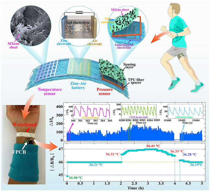
This is a preview of subscription content, log in via an institution to check access.
Access this article
Price includes VAT (Russian Federation)
Instant access to the full article PDF.
Rent this article via DeepDyve
Institutional subscriptions
Data availability
The data are available from the corresponding authors on reasonable request.
Bae GY, Pak SW, Kim D, Lee G, Kim DH, Chung Y, Cho K. Linearly and highly pressure-sensitive electronic skin based on a bioinspired hierarchical structural array. Adv Mater . 2016 ; 28 :5300–6.
Article CAS PubMed Google Scholar
Li Z, Zhu M, Shen J, Qiu Q, Yu J, Ding B. All-fiber structured electronic skin with high elasticity and breathability. Adv Funct Mater . 2020 ; 30 :1908411.
Article CAS Google Scholar
Cao Y, Tan YJ, Li S, Lee WW, Guo H, Cai Y, Wang C, Tee BCK. Self-healing electronic skins for aquatic environments. Nat Electron . 2019 ; 2 :75–82.
Article Google Scholar
Sun G, Wang P, Jiang Y, Sun H, Liu T, Li G, Yu W, Meng C, Guo S. Bioinspired flexible, breathable, waterproof and self-cleaning iontronic tactile sensors for special underwater sensing applications. Nano Energy . 2023 ; 110 : 108367.
Wang P, Li G, Liu J, Hou Z, Meng C, Guo S. Flexible, freestanding, ultrasensitive, and iontronic tactile sensing textile. ACS Appl Electron Mater . 2021 ; 3 :2195–202.
Libanori A, Chen G, Zhao X, Zhou Y, Chen J. Smart textiles for personalized healthcare. Nat Electro . 2022 ; 5 :142–56.
Wang Y, Jin J, Lu Y, Mei D. 3D printing of liquid metal based tactile sensor for simultaneously sensing of temperature and forces. Int J Smart Nano Mater . 2021 ; 12 :269–85.
Yan T, Wu Y, Tang J, Pan Z. Flexible strain sensors fabricated using aligned carbon nanofiber membranes with cross-stacked structure for extensive applications. Int J Smart Nano Mater . 2022 ; 13 :432–46.
Min J, Demchyshyn S, Sempionatto JR, Song Y, Hailegnaw B, Xu C, Yang Y, Solomon S, Putz C, Lehner LE, Schwarz JF, Schwarzinger C, Scharber MC, Shirzaei Sani E, Kaltenbrunner M, Gao W. An autonomous wearable biosensor powered by a perovskite solar cell. Nat. Electron . 2023 ; 6 : 630–41.
Zhang Y, Chen C, Qiu Y, Ma L, Qiu W, Yu R, Yu W, Liu XY. Meso-reconstruction of silk fibroin based on molecular and nano-templates for electronic skin in medical applications. Adv Funct Mater . 2021 ; 31 :2100150.
Lei D, Zhang Q, Liu N, Su T, Wang L, Ren Z, Zhang Z, Su J, Gao Y. Self-powered graphene oxide humidity sensor based on potentiometric humidity transduction mechanism. Adv Funct Mater . 2022 ; 32 :2107330.
Li X, Fan YJ, Li HY, Cao JW, Xiao YC, Wang Y, Liang F, Wang HL, Jiang Y, Wang ZL, Zhu G. Ultracomfortable hierarchical nanonetwork for highly sensitive pressure sensor. ACS Nano . 2020 ; 14 :9605–12.
Cao M, Su J, Fan S, Qiu H, Su D, Li L. Wearable piezoresistive pressure sensors based on 3D graphene. Chem Eng J . 2021 ; 406 : 126777.
Yan J, Ma Y, Li X, Zhang C, Cao M, Chen W, Luo S, Zhu M, Gao Y. Flexible and high-sensitivity piezoresistive sensor based on MXene composite with wrinkle structure. Ceram Int . 2020 ; 46 :23592–8.
Zhang W, Xiao Y, Duan Y, Li N, Wu L, Lou Y, Wang H, Peng Z. A high-performance flexible pressure sensor realized by overhanging cobweb-like structure on a micropost array. ACS Appl Mater Inter . 2020 ; 12 :48938–47.
Yin R, Li L, Wang L, Lou Z. Self-healing Au/PVDF-HFP composite ionic gel for flexible underwater pressure sensor. J Semicond . 2023 ; 44 :032602.
Shi Y, Zhang Z, Huang Q, Lin Y, Zheng Z. Wearable sweat biosensors on textiles for health monitoring. J Semicond . 2023 ; 44 :021601.
Lee J, Kwon H, Seo J, Shin S, Koo JH, Pang C, Son S, Kim JH, Jang YH, Kim DE, Lee T. Conductive fiber-based ultrasensitive textile pressure sensor for wearable electronics. Adv Mater . 2015 ; 27 :2433–9.
Durukan MB, Cicek MO, Doganay D, Gorur MC, Çınar S, Unalan HE. Multifunctional and physically transient supercapacitors, triboelectric nanogenerators, and capacitive sensors. Adv Funct Mater . 2022 ; 32 :2106066.
Lv C, Tian C, Jiang J, Dang Y, Liu Y, Duan X, Li Q, Chen X, Xie M. Ultrasensitive linear capacitive pressure sensor with wrinkled microstructures for tactile perception. Adv Sci . 2023 ; 10 :2206807.
Kim N-I, Chen J, Wang W, Moradnia M, Pouladi S, Kwon M-K, Kim J-Y, Li X, Ryou J-H. Highly-sensitive skin-attachable eye-movement sensor using flexible nonhazardous piezoelectric thin film. Adv Funct Mater . 2021 ; 31 :2008242.
Chorsi MT, Curry EJ, Chorsi HT, Das R, Baroody J, Purohit PK, Ilies H, Nguyen TD. Piezoelectric biomaterials for sensors and actuators. Adv Mater . 2019 ; 31 :1802084.
Maurya D, Khaleghian S, Sriramdas R, Kumar P, Kishore RA, Kang MG, Kumar V, Song H-C, Lee S-Y, Yan Y, Park J-M, Taheri S, Priya S. 3D printed graphene-based self-powered strain sensors for smart tires in autonomous vehicles. Nat Comm . 2020 ; 11 :5392.
Lu D, Liu T, Meng X, Luo B, Yuan J, Liu Y, Zhang S, Cai C, Gao C, Wang J, Wang S, Nie S. Wearable triboelectric visual sensors for tactile perception. Adv Mater . 2023 ; 35 :2209117.
Niu F, Qin Z, Min L, Zhao B, Lv Y, Fang X, Pan K. Ultralight and hyperelastic nanofiber-reinforced MXene–graphene aerogel for high-performance piezoresistive sensor. Adv Mater Technol-us . 2021 ; 6 :2100394.
Yang Z, Li H, Zhang S, Lai X, Zeng X. Superhydrophobic MXene@carboxylated carbon nanotubes/carboxymethyl chitosan aerogel for piezoresistive pressure sensor. Chem Eng J . 2021 ; 425 : 130462.
Wang C, Xia K, Wang H, Liang X, Yin Z, Zhang Y. Advanced carbon for flexible and wearable electronics. Adv Mater . 2019 ; 31 :1801072.
Li J, Yin J, Wee MGV, Chinnappan A, Ramakrishna S. A self-powered piezoelectric nanofibrous membrane as wearable tactile sensor for human body motion monitoring and recognition. Adv Fiber Mater . 2023 ; 5 :1417–30.
Ma J, Cui Z, Du Y, Zhang J, Sun C, Hou C, Zhu N. Wearable fiber-based supercapacitors enabled by additive-free aqueous MXene inks for self-powering healthcare sensors. Adv Fiber Mater . 2022 ; 4 :1535–44.
Liu S, Zhang W, He J, Lu Y, Wu Q, Xing M. Fabrication techniques and sensing mechanisms of textile-based strain sensors: from spatial 1D and 2D perspectives. Adv. Fiber Mater . 2024 ; 6 : 36–67.
Liu Z, Zhu T, Wang J, Zheng Z, Li Y, Li J, Lai Y. Functionalized fiber-based strain sensors: pathway to next-generation wearable electronics. Nano-Micro Lett . 2022 ; 14 :61.
Salvo P, Calisi N, Melai B, Cortigiani B, Mannini M, Caneschi A, Lorenzetti G, Paoletti C, Lomonaco T, Paolicchi A, Scataglini I, Dini V, Romanelli M, Fuoco R, Di Francesco F. Temperature and pH sensors based on graphenic materials. Biosens Bioelectron . 2017 ; 91 :870–7.
Gu Y, Hao J, Wu T, Zhang Z, Zhang Z, Li Q. Bimetallic MoNi/WNi nanoalloys for ultra-sensitive wearable temperature sensors. J Mater Chem A . 2022 ; 10 :5402–9.
Daus A, Jaikissoon M, Khan AI, Kumar A, Grady RW, Saraswat KC, Pop E. Fast-response flexible temperature sensors with atomically thin molybdenum disulfide. Nano Lett . 2022 ; 22 :6135–40.
Taroni PJ, Santagiuliana G, Wan K, Calado P, Qiu M, Zhang H, Pugno NM, Palma M, Stingelin-Stutzman N, Heeney M, Fenwick O, Baxendale M, Bilotti E. Toward stretchable self-powered sensors based on the thermoelectric response of PEDOT:PSS/Polyurethane blends. Adv Funct Mater . 2018 ; 28 :1704285.
Cao Z, Yang Y, Zheng Y, Wu W, Xu F, Wang R, Sun J. Highly flexible and sensitive temperature sensors based on Ti3C2Tx (MXene) for electronic skin. J Mater Chem A . 2019 ; 7 :25314–23.
Lin Y, Chen J, Tavakoli MM, Gao Y, Zhu Y, Zhang D, Kam M, He Z, Fan Z. Printable fabrication of a fully integrated and self-powered sensor system on plastic substrates. Adv Mater . 2019 ; 31 :1804285.
Zhang Q, Lei D, Liu N, Liu Z, Ren Z, Yin J, Jia P, Lu W, Gao Y. A zinc-ion battery-type self-powered pressure sensor with long service life. Adv Mater . 2022 ; 34 :2205369.
Park H, Song C, Jin SW, Lee H, Keum K, Lee YH, Lee G, Jeong YR, Ha JS. High performance flexible micro-supercapacitor for powering a vertically integrated skin-attachable strain sensor on a bio-inspired adhesive. Nano Energy . 2021 ; 83 : 105837.
Song Y, Chen H, Chen X, Wu H, Guo H, Cheng X, Meng B, Zhang H. All-in-one piezoresistive-sensing patch integrated with micro-supercapacitor. Nano Energy . 2018 ; 53 :189–97.
Chen X, Hou Z, Li G, Yu W, Xue Y, Niu G, Xin M, Yang L, Meng C, Guo S. A laser-scribed wearable strain sensing system powered by an integrated rechargeable thin-film zinc–air battery for a long-time continuous healthcare monitoring. Nano Energy . 2022 ; 101 : 107606.
Yu Y, Nassar J, Xu C, Min J, Yang Y, Dai A, Doshi R, Huang A, Song Y, Gehlhar R, Ames AD, Gao W. Biofuel-powered soft electronic skin with multiplexed and wireless sensing for human-machine interfaces. Sci Robot . 2020 ; 5 :eaaz7946.
Article PubMed PubMed Central Google Scholar
Song Y, Min J, Yu Y, Wang H, Yang Y, Zhang H, Gao W. Wireless battery-free wearable sweat sensor powered by human motion. Sci Adv . 2020 ; 6 :eaay9842.
Article CAS PubMed PubMed Central Google Scholar
Meng K, Zhao S, Zhou Y, Wu Y, Zhang S, He Q, Wang X, Zhou Z, Fan W, Tan X, Yang J, Chen J. A wireless textile-based sensor system for self-powered personalized health care. Matter . 2020 ; 2 :896–907.
Xu F, Dong S, Liu G, Pan C, Guo ZH, Guo W, Li L, Liu Y, Zhang C, Pu X, Wang ZL. Scalable fabrication of stretchable and washable textile triboelectric nanogenerators as constant power sources for wearable electronics. Nano Energy . 2021 ; 88 : 106247.
Yin L, Kim KN, Lv J, Tehrani F, Lin M, Lin Z, Moon J-M, Ma J, Yu J, Xu S, Wang J. A self-sustainable wearable multi-modular E-textile bioenergy microgrid system. Nat Commun . 2021 ; 12 :1542.
Manthiram A. A reflection on lithium-ion battery cathode chemistry. Nat Comm . 2020 ; 11 :1550.
Kim T, Song W, Son D-Y, Ono LK, Qi Y. Lithium-ion batteries: outlook on present, future, and hybridized technologies. J Mater Chem A . 2019 ; 7 :2942–64.
Liu S, Ji H, Wang M, Sun H, Liu J, Yan C, Qian T. Atomic metal vacancy modulation of single-atom dispersed Co/N/C for highly efficient and stable air cathode. ACS Appl Mater Inter . 2020 ; 12 :15298–304.
Hou Z, Zhu B, Li G, Wang P, Meng C, Guo S, Liu C, Fan S. Nanostructured Co3O4 asymmetrically deposited on a single carbon cloth for an all-solid-state integrated hybrid device with reversible zinc–air high-energy conversion and asymmetric supercapacitive high-power delivery. Energ Fuel . 2021 ; 35 :12706–17.
Fang W, Zhao J, Zhang W, Chen P, Bai Z, Wu M. Recent progress and future perspectives of flexible Zn-Air batteries. J Alloy Compd . 2021 ; 869 : 158918.
Wang M, Ji H, Liu S, Sun H, Liu J, Yan C, Qian T. Single-atom scale metal vacancy engineering in heteroatom-doped carbon for rechargeable zinc–air battery with reduced overpotential. Chem Eng J . 2020 ; 393 : 124702.
Huang Y, Liu B, Zhang W, Qu G, Jin S, Li X, Nie Z, Zhou H. Highly sensitive active-powering pressure sensor enabled by integration of double-rough surface hydrogel and flexible batteries. Npj Flex Electron . 2022 ; 6 :92.
Sun B, McCay RN, Goswami S, Xu Y, Zhang C, Ling Y, Lin J, Yan Z. Gas-permeable, multifunctional on-skin electronics based on laser-induced porous graphene and sugar-templated elastomer sponges. Chem Eng J . 2018 ; 30 :1804327.
Google Scholar
Download references
Acknowledgements
This research was supported by the National Natural Science Foundation of China under Grant (62174068), the Tianjin Science and Technology Plan Project (22JCZDJC00630), the Higher Education Institution Science and Technology Research Project of Hebei Province (JZX2024024), the China National Key Research and Development Program (2022YFC3601400), and the Natural Science Foundation of Shandong Province China, (ZR2020ME120).
This article is funded by National Natural Science Foundation of China, 62174068, Yang Li, Tianjin Municipal Science and Technology Program, 22JCZDJC00630, Chuizhou Meng, China National Key Research and Development Program, 2022YFC3601400, Chuizhou Meng, Science and Technology Innovative Research Team in Higher Educational Institutions of Hunan Province, JZX2024024, Chuizhou Meng, Natural Science Foundation of Shandong Province, ZR2020ME120.
Author information
Authors and affiliations.
School of Mechanical Engineering, University of Jinan, Jinan, 250022, China
State Key Laboratory for Reliability and Intelligence of Electrical Equipment, Engineering Research Center of Ministry of Education for Intelligent Rehabilitation Device and Detection Technology, Hebei Key Laboratory of Smart Sensing and Human-Robot Interaction, School of Mechanical Engineering, Hebei University of Technology, Tianjin, 300401, China
Gengsheng Liu, Guifen Sun & Chuizhou Meng
School of Integrated Circuits and Electronics, Beijing Institute of Technology, Beijing, 100081, China
Guozhen Shen
Shandong Provincial Key Laboratory of Network Based Intelligent Computing, School of Information Science and Engineering, University of Jinan, Jinan, 250022, China
School of Microelectronics, Shandong University, Jinan, 250101, China
You can also search for this author in PubMed Google Scholar
Corresponding authors
Correspondence to Chuizhou Meng , Guozhen Shen or Yang Li .
Ethics declarations
Conflict of interest.
The authors state that there are no conflicts of interest to disclose.
Additional information
Publisher's note.
Springer Nature remains neutral with regard to jurisdictional claims in published maps and institutional affiliations.
Supplementary Information
Below is the link to the electronic supplementary material.
Supplementary file1 (DOCX 4343 KB)
Supplementary file2 (MP4 5686 KB)
Supplementary file3 (MP4 8532 KB)
Supplementary file4 (MP4 5809 KB)
Rights and permissions
Springer Nature or its licensor (e.g. a society or other partner) holds exclusive rights to this article under a publishing agreement with the author(s) or other rightsholder(s); author self-archiving of the accepted manuscript version of this article is solely governed by the terms of such publishing agreement and applicable law.
Reprints and permissions
About this article
Wang, P., Liu, G., Sun, G. et al. An Integrated Bifunctional Pressure‒Temperature Sensing System Fabricated on a Breathable Nanofiber and Powered by Rechargeable Zinc–Air Battery for Long-Term Comfortable Health Care Monitoring. Adv. Fiber Mater. (2024). https://doi.org/10.1007/s42765-024-00398-5
Download citation
Received : 28 November 2023
Accepted : 19 February 2024
Published : 11 April 2024
DOI : https://doi.org/10.1007/s42765-024-00398-5
Share this article
Anyone you share the following link with will be able to read this content:
Sorry, a shareable link is not currently available for this article.
Provided by the Springer Nature SharedIt content-sharing initiative
- Pressure‒temperature sensor
- Rechargeable zinc–air battery
- Electrospun nanofibers
- Permeable electronic
- Integrated sensing system
- Find a journal
- Publish with us
- Track your research

An official website of the United States government
The .gov means it’s official. Federal government websites often end in .gov or .mil. Before sharing sensitive information, make sure you’re on a federal government site.
The site is secure. The https:// ensures that you are connecting to the official website and that any information you provide is encrypted and transmitted securely.
- Publications
- Account settings
Preview improvements coming to the PMC website in October 2024. Learn More or Try it out now .
- Advanced Search
- Journal List
- Nanomaterials (Basel)
An Ultrahigh Sensitive Paper-Based Pressure Sensor with Intelligent Thermotherapy for Skin-Integrated Electronics
1 State Key Laboratory of Electronic Thin Films and Integrated Devices, School of Optoelectronic Science and Engineering, University of Electronic Science and Technology of China (UESTC), Jianshe North Road, Chengdu 610054, China; moc.361@udeoag_nil (L.G.); nc.ude.ctseu@uysj (J.Y.)
2 Research Institute for New Materials Technology, Chongqing University of Arts and Sciences, Honghe Avenue, Chongqing 402160, China; moc.361@gnawnewp (P.W.); moc.361@669945719s (J.S.); moc.361@432151yxd (X.D.)
Junsheng Yu
Peiwen wang, xiaoyan deng, associated data.
Porous microstructure pressure sensors that are highly sensitive, reliable, low-cost, and environment-friendly have aroused wide attention in intelligent biomedical diagnostics, human–machine interactions, and soft robots. Here, an all-tissue-based piezoresistive pressure sensor with ultrahigh sensitivity and reliability based on the bottom interdigitated tissue electrode and the top bridge of a microporous tissue/carbon nanotube composite was proposed. Such pressure sensors exhibited ultrahigh sensitivity (≈1911.4 kPa −1 ), fast response time (<5 ms), low fatigue of over 2000 loading/unloading cycles, and robust environmental degradability. These enabled sensors can not only monitor the critical physiological signals of the human body but also realize electrothermal conversion at a specific voltage, which enhances the possibility of creating wearable thermotherapy electronics for protecting against rheumatoid arthritis and cervical spondylosis. Furthermore, the sensor successfully transmitted wireless signals to smartphones via Bluetooth, indicating its potential as reliable skin-integrated electronics. This work provides a highly feasible strategy for promoting high-performance wearable thermotherapy electronics for the next-generation artificial skin.
1. Introduction
Pressure sensors, which convert pressure signals into electrical signals, offer a variety of existing and emerging applications, such as soft robots, human–machine interfaces, medical diagnostics, and artificial intelligences, among many others [ 1 , 2 , 3 , 4 , 5 , 6 ]. For instance, such sensors can be spontaneously mounted on a dynamic and curved epidermis to detect the body’s vital physiological mechanical signals through real-time transmissions, thus realizing wearable Internet of Things in society [ 7 , 8 , 9 , 10 ]. At present, piezoelectric [ 11 ], piezoresistive [ 12 , 13 ], triboelectric [ 14 , 15 ], and capacitive [ 16 , 17 ] pressure sensing mechanisms and functional materials with multivariant microstructure collocation strategies have converged to meet the requirements of next-generation wearable electronics. Taking the manufacturing cost, sensitivity, response time, reliability, and large-area array process into consideration, a piezoresistive device is regarded as an attractive choice for next-generation pressure sensors.
In recent years, substantial breakthroughs have been made in relevant research, the first is to select various highly conductive materials as pressure-sensing elements, such as conductive polymers [ 18 , 19 , 20 ], carbon materials [ 21 , 22 , 23 , 24 , 25 , 26 ], metal nanowires [ 27 , 28 , 29 ], and two-dimensional materials [ 30 ]. The second is to design sophisticated microstructures to induce conductive contact enhancement, mainly including common porous structures [ 31 ], micropyramid structures [ 32 ], microdome structures [ 33 ], micropillar structures [ 34 ], and so forth. Although these microstructures have been optimized and improved continuously by multiple technologies, the complicated harsh and time-consuming fabrication processes are always neglected, limiting their practical applications to a certain extent. Consequently, pressure sensors with a facile, low-cost, and environment-friendly method must be dominant choices, and one feasible approach to realize that is through paper-based wearable electronic devices [ 35 , 36 ]. The natural properties and porous microstructure of the paper provide the basic conditions for the realization of high-performance pressure sensors [ 37 ]. Some recent studies demonstrated that the conductive materials of a paper-based pressure sensor were embedded into the microstructure fiber paper using various preparation processes [ 38 , 39 , 40 , 41 , 42 , 43 , 44 , 45 , 46 ]. For example, Tao et al. proposed a pressure sensor fabricated by mixing the tissue paper with graphene oxide solution, whose performance indicated a pressure range of 20 kPa and a high sensitivity of 17.2 kPa −1 (0−2 kPa) [ 41 ]. Guo et al. prepared a sensitive and degradable pressure sensor by sandwiching a porous Ti 3 C 2 T x tissue paper between a biodegradable polylactic acid (PLA) and an interdigitated electrode-coated PLA [ 42 ]. Similarly, Han et al. stacked the irregular surface and fiber network structure of multilayer carbon black and air-laid paper to increase the number of electrical contact points under pressure, which contributed to prominent performances of the pressure sensors [ 43 ]. Even if great progress was made in paper-based pressure sensors, the application is more limited to the detection of basic physiological signals and lacks depth extension, incapable of combining electrothermal properties with mechanical durability for thermotherapy application. Therefore, simultaneously achieving reliable pressure integrity and competent electrothermal properties for fabricating multifunctional smart paper-based electronics for both physiological signal monitoring and thermotherapy application is highly desired, but it remains challenging.
In this paper, we introduced a low-cost, environment-friendly, skin-comfortable, and air-permeable soft tissue as the backbone (sensitive layer and flexible substrate) to monitor microvibration physiological signals and realize pressure-regulated intelligent thermotherapy applications. The ultrahigh sensitivity and fast response time realized by the immersion process of tissue and aqueous carbon nanotube (CNT) solutions are the best results reported for paper-based pressure sensors. The spontaneous interaction between CNTs and paper fibers contributes to the formation of reliable conductive networks and robust mechanical properties. Finally, an optimized sensor was deployed on a Bluetooth module that transmits wireless signals to a smartphone. This work opens up more possibilities for practical applications in soft robots, electronic skins, intelligent healthcare, and artificial intelligence.
2. Experimental Section
Material Preparation: Aqueous dispersion of CNTs was purchased from XFNANO (Nanjing, China) for conductive materials. Clean and soft tissue ( Figure S1a ) was used as flexible substrates and the backbone of sensitive layers. Conductive sliver paste was used as bottom electrodes. Additionally, VHB film (3M VHB Tape 4910, St. Paul, MN, USA) was used to assemble the sensor.
Device Fabrication: The soft, clean tissue was first immersed in the aqueous dispersion of CNTs for 30 s, which ensured that CNTs effectively diffused through the microporous structure and uniformly adhered to the fibers in the diffusion path. Then, the tissue/CNT composites were transferred into an oven and dried at 70 °C for 2 h to evaporate the water solvent. Meanwhile, the conductive track circuit was prepared on the flexible tissue substrate by screen printing method. To form stable and low square resistance electrodes, the silver paste was scraped three to five times along the same direction on the designed screen, followed by a drying process in the oven for 2 h. The silver electrodes coated on the tissue substrate with a sheet resistance of ≈0.42 Ω sq −1 are described in Figure S1 . Finally, ultrathin VHB tape was used to assemble the two functional layers to form integral pressure sensors.
Measurement and Characterization: The surface morphologies of the tissue and tissue/CNT composites were characterized by field-emission SEM (GeminiSEM 300, Hallbergmoos, Germany)). The morphology of the silver paste electrode on the tissue was observed by microscopy. The 3D surface profile of the CNT-immersed tissue was characterized by laser scanning confocal microscopy (OPTELICS C130, Kanagawa, Japan). An FTIR (VERTEX 80v, Bruker, Karlsruhe, Germany) spectrometer was used to measure the infrared spectra of samples. The mechanical and electrical behaviors were analyzed via the combination of a mechanical test analyzer (TestStar ETM102B-TS, Shenzhen, China) and electrochemical workstation (CHI 760E, Shanghai, China). Additionally, a digital source meter (Keithley 2400, Beaverton, OR, USA) was used to measure the sheet resistance of the different samples.
3. Result and Discussion
3.1. structural design and composition characterization of all-tissue pressure sensors.
The all-soft-tissue-based pressure sensor consists of two functional layers, the top tissue/CNT composites for pressure sensing and the bottom tissue with conductive electrode acting as flexible substrate and skin contact. The fabrication procedures for the pressure sensors are illustrated in Figure 1 . Such sensor not only has reliable device structure, low-cost material selection, and facile fabrication process but also can be conveniently attached to the human epidermis with skin comfortability and air breathability.

Schematic illustration of the fabrication procedure of all-tissue-based pressure sensors.
The SEM images in Figure S2 and Figure 2 a–c show the surface morphologies of tissue and tissue/CNT composites. The tissue with a natural porous structure was mainly made of randomly interconnected cellulose, which facilitated the diffusion of aqueous solutions and the attachment of conductive materials ( Figure S2 ). The uniformity of CNTs can be guaranteed through the staggered adhesion on the fibers; thus the internal porous structures and the top-down cascaded fiber contact boost the sensitivity under pressure. It is worth noting that CNTs did not cover the original porosity of the tissue during the immersion process, and the excellent air permeability contributed to the integration with human skins ( Figure 2 ). FTIR spectroscopy was performed to reveal the chemical bonds between the tissue and CNTs ( Figure 2 d). The vibration peaks of the CNTs were induced by surface modification, which conduced to the stable dispersion in aqueous solution. The typical characteristic peaks of a tissue at 1027.80, 2897.49, and 3331.53 cm −1 can be assigned to the stretching vibration of C–O–C, C–H, and –OH groups. Additionally, a series of vibrations were red-shifted to 1023.63, 2893.43, and 3293.70 cm −1 , indicating that a chemical interaction existed between the tissue and CNTs. Therefore, the coupling process is conducive to improving the reliability of pressure sensors. Besides, the 3D surface profile ( Figure 2 e,f) was further employed to reveal the overall distributions of the spiny microstructure formed by interlaced fibers, and provides a certain height range of the random distribution of the spiny microstructure for electrical contact reinforcement.

Composition characterization of the all-tissue-based pressure sensor. ( a , b ) Surface morphology of tissue/CNT composites. ( c ) Adhesion of CNTs to a single fiber. ( d ) FTIR results of CNT, tissue, and tissue/CNT composites. ( e ) 3D surface profile of tissue/CNT composites. ( f ) The proportion distribution of the surface roughness.
3.2. Pressure-Sensing and Electrothermal-Converting Properties of the Porous Tissue-Based Sensor
The first consideration is whether the pressure sensor complies with Ohm’s law for skin-integrated piezoresistive devices. Figure 3 a presents the current-voltage (I−V) curves with voltage scanning from −0.5 to 0.5 V for an all-facial-tissue-based sensor, and the linear dependence of voltage on current at various applied pressures clearly shows that there is good ohmic contact between the top sensitive layer and the bottom printed electrode. The pressure-sensing characteristics of different tissue laminations are shown in Figure 3 b. The calculation of sensitivity was derived from the formula S = δ(ΔI/I 0 )/δP, where ΔI refers to the relative change in current, I 0 refers to the initial current, and δP refers to the change of applied pressure. Apparently, the sensitivity of the sensor can be categorized into two regions: an ultrahigh sensitive region and a normal sensitive region, which are highly dependent on the number of tissue layers. Among them, the triple-layered tissue exhibits an ultrahigh sensitivity of 1911.4 kPa −1 (even the single-layered tissue reaches up to 428.4 kPa −1 ), which is the highest value of paper-based pressure sensors. The reasons for the significant differences in the number of layers of sensitive materials are further explored. On the one hand, the microscopic wrinkles on the surface of the tissue lead to the spontaneous formation of microstructure air gaps between layers, and these microgaps intuitively indicate that the sensor is sensitive to small external pressures [ 41 ]. The compressive stress was measured to assess the mechanical properties of the composite film ( Figure S3 ). Both of the tissues with and without CNTs were capable of deforming mechanically up to 50% under a pressure of 9 kPa, which indicates that the tissue-based sensor is soft enough and prone to deformation. We define an effective elastic modulus (E eff ) as the slope of the stress versus the strain plot, which is directly influenced by the morphology, roughness, and material properties of the sensitive layer. Both the intrinsic tissue and the composite showed an approximate elastic modulus (≈20.0 kPa), which was also much lower than that of other flexible materials, such as cotton (≈73.6 kPa) [ 20 ] and PDMS (≈200 kPa) [ 18 ]. On the other hand, a favorable conductive pathway was formed when the CNTs diffused through the microporous structure and adhered to the fibers of the tissue during the immersion process ( Figure 2 b,c), and the increase of stacked layers also reduced the square resistance ( Figure 3 c), thus enhancing the current to realize ultrahigh sensitivity.

Pressure sensing and electrothermal converting of all-tissue-based electronics. ( a ) Current-voltage (I−V) curves of the sensor with various applied pressures. ( b ) Relative current changes and sensitivity of the sensor. ( c ) Sheet resistance of various tissue layers. ( d ) Response times (rise time and decay time) of the sensor. ( e ) Current-time (I–t) curves of the sensor under serial continuous pressure changes. ( f ) The durability test of the sensor in a pressure range of 1–2 kPa. ( g ) Time-dependent temperature variation with applied voltage. ( h ) Temperature profiles under a stepwise voltage from 1–6 V. ( i ) Temperature–time curve under a 5 V input voltage for 10 cycles.
In addition, another important criterion for real-time human–machine interaction through pressure sensors is dynamic response, especially the rise and decay time during the process of applying and withdrawing mechanical pressure. As shown in Figure 3 d, the rise and decay time are 4 and 3 ms, respectively. Such a rapid response time is sufficient to respond to continuous external pressures. Hence, various degrees of pressure were applied to the sensor, and the results are presented in Figure 3 e, indicating that the tissue-based sensor has good reliability and can intelligently perceive and distinguish pressure changes. Periodic cyclic compression experimental tests were conducted to further explore the remarkable performance robustness of the soft-tissue-based pressure sensor. As shown in Figure 3 f, the device demonstrated excellent cyclic stability without any evident fatigue in 10,000 s (≈2000 cycles). Notably, all-tissue-based flexible pressure sensors have the promising potential to resolve the issue of electronic waste depending on their biodegradable ability and outstanding biocompatibility, which is described in the combustion process shown in Figure S4 and Video S1 .
The high performance of an all-tissue-based pressure sensor is mainly attributed to the internal porous microstructures of the tissue, the microfolds on the laminated surfaces, the high intrinsic conductivity of CNTs, and the spontaneous formation of stable conduction pathways. The work was compared meticulously with other paper-based pressure sensors as shown in Table 1 . Obviously, both sensitivity and response time are the best results currently available based on paper-based pressure sensors, and sensitivity greatly increased about 37 times.
Comparison of all research studies about paper-based pressure sensors.
With the excellent electrical conductivity of CNTs, all-tissue-based pressure sensors demonstrated tremendous intelligent thermotherapy application by utilizing the Joule heating effect. As illustrated in Figure 3 g, the tissue and CNT composite films exhibit an obviously electrothermal conversion phenomenon, which can reach the equilibrium temperature and recover the initial state in a very short time (both are less than 10 s). The equilibrium temperature generated in this process is derived from the Joule heating effect, which relies on the applied voltage. The temperature can also be correspondingly varied by continuous regulation of voltage ( Figure 3 h), indicating that films have excellent adjustability in thermotherapy applications. The cyclic thermal response results at an input voltage of 5 V are shown in Figure 3 i. A temperature from 23 to 58 °C can be regulated in 10 cycles, proving the outstanding durability under an ambient condition for long-term use. To further evaluate the relationship between the pressure, temperature, and resistance of the all-tissue-based sensor, the temperature–current curve of the sensor under constant pressure loading was measured ( Figure S5a ), and the current variation of temperature induced was negligible with respect to the regulation of pressure. The pressure-regulated heating properties of the sensor were characterized as pressure–temperature functions under various voltages ( Figure S5b ), which indicates that the temperature can be manipulated via mechanical pressure from room temperature (19 °C) to designated application temperatures. Consequently, such sensors, combined with electrothermal conversion, provide a very dominant choice for the popularization and application of skin-integrated electronic products.
3.3. Human Physiological Signals Monitoring and Intelligent Thermally Management
The skin surface of a human is a tactile perception system with unique physiological signal signatures for different parts. Based on their ultrahigh pressure sensitivity, fast response time, and conformal ability, all-facial-tissue-based pressure sensors are capable of monitoring all forms of human physical action and some physiological signals in a fast, real-time, noninvasive, and user-interactive way for applications, such as e-skins, medical treatment, and artificial intelligence.
Generally, it is imperative to maintain the close contact between the pressure sensor and the human skin for subtle monitoring, and the pre-force that exists has almost no effect on the signal acquisition, so the sensor is attached to the corresponding body parts with the aid of a biocompatible woundplast. As presented in Figure 4 a–h, the sensor can be installed in various parts of the human body, such as the finger, joints, chest, and throat, indicating a perfect interaction with the human skin. By touching the sensor with different finger forces ( Figure 4 a), the results showed significant relative changes, whether gently touched or pressed, which facilitates the integration into human skin to distinguish external force information in real time. Joint motion is also detectable, such as knee bending angle. Knee bending tests of 10, 30, 60, and 90 degrees were conducted ( Figure 4 h), and high current stability was realized by bending the sensor at different angles so that it is highly robust to monitor frequent human motion.

Schematic illustration of human motion and physiological signal monitoring of the pressure sensor. ( a ) Diagram of a sensor touched with various forces. ( b ) Real-time monitoring of the radial artery normal pulse by attaching a sensor to the wrist. ( c ) Exercise pulse test after 1 min of plank. ( d ) Normal breath and deep breath mode test by attaching a sensor to the chest. ( e – g ) Voice recognition by mounting a sensor on the throat to detect vocal cord vibrations. ( h ) Detection of leg swing angles by attaching a sensor to the knee.
The heart rate (pulse) is often used as one of the important vital signs to assess a person’s physical and mental condition. A large amount of blood entering the arteries increases the pressure and enlarges the diameter of the arteries, which can be felt on the shallow surface of the body, especially the wrist. The pulse beat under normal condition and after 1 min of plank was measured, and the results are shown in Figure 4 b,c. The pulse beats changed from 12 in the normal state to 14 in the exercise state, translating into 72 and 84 beats per minute, respectively. Additionally, the current variation increased from 20 to 40 μA with each pulse beating. Hence, the above results show that exercise can enhance the heart rate and intensity, and the sensor has a certain medical diagnostic ability. Furthermore, the frequency waveforms of normal and deep breathing were tested ( Figure 4 d), and the contraction and relaxation of the chest can be directly captured, which is one of the major applications of e-skins.
Moreover, voice recognition was realized by attaching the sensor to the throat to distinguish various words or phrases, such as “hello,” “sensor,” and “pressure sensor” ( Figure 4 e–g). Multiple readings of each word propagate a similar characteristic current signal, and the extended phrase of the word can also maintain general consistency. For example, when the phrase “pressure sensor” is said, the word “sensor” has the original two peak current signals, and perhaps the tone level and word conversion process can cause slight signal disturbances. Generally speaking, tissue-based pressure sensors with the ability of voice recognition not only are useful for the voice recovery of people with vocal cord damage but also promote the development human–machine interactions and artificial intelligence.
More importantly, adopting a pressure-regulated strategy realizes accurate electrothermal conversion, enhancing the great possibility of providing wearable thermotherapy (the therapeutic effect induced by heat), that is, rehabilitation of rheumatoid arthritis, regulation of joint stiffness, and improvement of blood circulation. Figure 5 a depicts the self-regulating form of temperature at various knuckle bending angles. Variable bending angles promote electrical contact enhancement to generate more Joule heat. This effect intuitively translates into a change in temperature. The heat generation of wearable electronics through the continuous movement of joints can achieve the effects of relaxing muscles and activating blood circulation in two ways (joint motion, thermotherapy), which is conducive to the rehabilitation of rheumatoid arthritis. Such wearable pressure sensors can also be used on important body parts, such as the cervical vertebra and lumbar vertebra ( Figure 5 b–d). For example, twisting the neck or moving the waist can realize the function of automatic thermotherapy. Consequently, wearable electronics can greatly relieve our work fatigue and prevent cervical spondylosis and other problems.

Thermotherapy applications and wireless real-time monitoring of the sensor. ( a ) Temperature dependent with various bending angles. ( b – d ) Temperature changes during cervical and lumbar spine twisting. ( e ) Wearable sensor system for wireless transmission and data storage function configuration. ( f ) Wireless function spread on touching mode. ( g ) Respiratory signals of mobile terminal by attaching the device to the chest.
Through the assembly of a tissue-based sensor and multifunctional integrated module ESP32 (Bluetooth, antenna, filter, power source, etc.) and programmed software writing and debugging, the wireless transmission and signal acquisition of portable smartphones were successfully realized ( Figure S6 ). The auto-stored data of pressure-applied and respiration process from the previous moment were taken out and are depicted in Figure 5 e–g. On the one hand, the random variation of pressure signals on touch mode indicates the controllability of the sensing system, and this sensor can wirelessly feedback the pressure condition of the external environment. On the other hand, 10 breaths in 30 s indicates some basic physical conditions of the human body, and such sensor can also wirelessly monitor physiological signals in real time. The continuous breath process is shown in Video S2 . Consequently, the systematic implementation of wireless data transmission and storage provides a crucial step for skin-integrated electronics, and the real-time feedback function lays a solid foundation for soft robotics, medical diagnostics, and artificial intelligence applications.
4. Conclusions
In this paper, pressure sensors with ultrahigh sensitivity were prepared by using an all-tissue-based backbone and integrating them with a Bluetooth module for wireless transmission. In particular, these sensors offer a sensitivity of up to 1911.4 kPa −1 , fast response time, outstanding reliability, and environmental degradability. Such all-tissue-based pressure sensors can be of value in many applications, including basic human motion detection, pulse detection, respiratory detection, and voice recognition. Through the thermal effect of pressure regulation, wearable thermotherapy electronics for protecting against rheumatoid arthritis and cervical spondylosis were further realized. It is anticipated that the sensor can easily provide a more scalable method for skin-integrated electronics to manufacture large-area thermotherapy pressure sensors.
Supplementary Materials
The following are available online at https://www.mdpi.com/2079-4991/10/12/2536/s1 . Figure S1: (a) Surface topography of tissue in microscope. (b) Bottom electrode after screen printing on tissue. (c,d) Adhesion of silver paste used in bottom electrode; Figure S2: SEM images about the surface morphologies of tissue. (a) Surface distribution. (b) Local distribution. (c) Single fiber distribution; Figure S3: Consecutive compression tests on the sensitive layer. (a) Intrinsic tissue. (b) Tissue and CNT composites; Figure S4: Degradation process of all tissue-based sensors. (a) Before combustion. (b,c) Combustion process. (d) Combustion degradation completed; Figure S5: (a) The temperature-current curve of pressure sensor under constant pressure loading (pressure: 2 kPa, voltage: 3 V). (b) The pressure-temperature functions under varies voltage; Figure S6: Schematic diagram of Bluetooth wireless system; Video S1: Combustion process of all tissue-based sensor; Video S2: Continuous breath process of wireless sensor.
Author Contributions
Conceptualization, Y.L. and L.G.; formal analysis, P.W.; investigation, J.S. and X.D.; methodology, Y.L. and L.G.; project administration, Y.L.; supervision, L.L.; writing—review and editing, J.Y. and Y.L. All authors have read and agreed to the published version of the manuscript.
This work was supported by the National Key Research and Development Project of China (Grant No. 2018YFB0407102), National Natural Science Foundation of China (Grant Nos. U1663229, 21603020, 61705026, and 51903026), Sichuan Science and Technology Program (Grant Nos. 2020YFG0281, 2020YFG0279, and 2019YFG0121), Chongqing Science and Technology Commission (Grant No. cstc2019jcyjjqx0021), Chongqing Science and Technology Innovation Leading Talent Support Program (Grant No. T04040012), Scientific and Technological Research Program of Chongqing Municipal Education Commission (Grant No. KJQN202001318), and Public Service Platform for the Industrialization of Technological Innovation Achievements in the Field of Robot and Intelligent Manufacturing in Chongqing (Grant No. 2019-00900-1-1). This study was also sponsored by the Sichuan Province Key Laboratory of Display Science and Technology.
Conflicts of Interest
There are no conflicts of interest to declare.
Ethics Statement
All subjects gave their informed consent for inclusion before they participated in the study. The study was conducted in accordance with the Declaration of Helsinki, and the protocol was approved by the Ethics Committee of Yongchuan Hospital, Chongqing Medical University (approval No. 201828).
Publisher’s Note : MDPI stays neutral with regard to jurisdictional claims in published maps and institutional affiliations.
Nanocellulose-Enhanced, Easily Processable Cellulose-Based Flexible Pressure Sensor for Wearable Epidermal Sensing
Affiliations.
- 1 State Key Laboratory of Pulp and Paper Engineering, South China University of Technology, Guangzhou 510641, China.
- 2 School of Chemistry and Chemical Engineering, South China University of Technology, Guangzhou 510641, China.
- 3 Zhejiang Jinjiahao Green Nanomaterials Co., Ltd., Quzhou 324404, China.
- PMID: 38597296
- DOI: 10.1021/acsami.4c03541
Flexible pressure sensors (FPSs) based on biomass materials have gained considerable attention for their potential in wearable electronics, human-machine interaction, and environmental protection. Herein, flexible silver nanowire-dual-cellulose paper (SNdCP) containing common cellulose fibers, cellulose nanofibers (CNFs), and silver nanowires (AgNWs) for FPSs was assembled by a facile papermaking strategy. Compared with bacterial cellulose (BC) and cellulose nanocrystals (CNCs), CNFs possess better dimensions and reinforcement, which enables the composite paper to exhibit better mechanical properties (tensile stress of 164.65 MPa) and electrical conductivity (11600 S·m -1 ), providing more possibilities for FPSs. Benefiting from these advantages, we construct an easily processable and sensitive human-interactive FPS based on a composite paper with high sensitivity (0.050 kPa -1 ), fast response/recovery time (158/95 ms), and exceptional stability (>1000 bending cycles), capable of responding to finger motions, voice recognition, and human pulses; through further employment as the array unit and a control circuit, the observed highly adaptive mechano-electric transformability and functions are well maintained. Overall, a facile and versatile strategy with the potential to provide clues for the fabrication of cellulose-based FPSs with outstanding performance was introduced.
Keywords: biomass materials; conductive paper; flexible pressure sensor; flexible substrate; nanocellulose.
High Sensitivity Photon Pressure Sensitive Skin of Piercing Robot Based on Balloon-Shaped Fiber Optic Sensor
Ieee account.
- Change Username/Password
- Update Address
Purchase Details
- Payment Options
- Order History
- View Purchased Documents
Profile Information
- Communications Preferences
- Profession and Education
- Technical Interests
- US & Canada: +1 800 678 4333
- Worldwide: +1 732 981 0060
- Contact & Support
- About IEEE Xplore
- Accessibility
- Terms of Use
- Nondiscrimination Policy
- Privacy & Opting Out of Cookies
A not-for-profit organization, IEEE is the world's largest technical professional organization dedicated to advancing technology for the benefit of humanity. © Copyright 2024 IEEE - All rights reserved. Use of this web site signifies your agreement to the terms and conditions.
IMAGES
VIDEO
COMMENTS
Moreover, this paper presents a comprehensive review on the present trend of research on MEMS-. based pressure sensors, their applications, and the research gap observed to date along with the ...
This paper reviews common new trends in MEMS pressure sensors, including minute differential pressure sensors (MDPSs), resonant pressure sensors (RPSs), integrated pressure sensors, miniaturized ...
In the pressure range of 0-2 kPa, the sensor sensitivity can be up to 17.2 kPa −1 and the response time is 60 ms. Furthermore, this new graphene paper-based sensor also has the advantages of environmental protection, low cost, high flexibility, simple preparation process and other outstanding advantages.
MEMS-based pressure sensors enable a wide range of pressure measurement as per the application requirements.,The paper provides a detailed review on fundamentals, classification and progresses in pressure sensors, along with its wide area of applications, its design aspects and challenges, to provide state of the art gist to the researchers of ...
Sensitivity (S) is used to assess the sensing performance of the pressure sensor under external pressure and is defined as, where I 0 is the initial current, ΔP is the pressure change, ΔI is the current change when the pressure change is ΔP. The application testing of the pressure sensor involves human health monitoring.
Flexible pressure sensors are attracting great interest from researchers and are widely applied in various new electronic equipment because of their distinct characteristics with high flexibility, high sensitivity, and light weight; examples include electronic skin (E-skin) and wearable flexible sensing devices. This review summarizes the research progress of flexible pressure sensors ...
Flexible piezoresistive pressure sensors have received great popularity in flexible electronics due to their simple structure and promising applications in health monitoring and artificial intelligence. However, the contradiction between sensitivity and detection range limits the application of the sensors in the medium-pressure regime. Here, a flexible piezoresistive pressure sensor is ...
With the continuous progress of aerospace, military technology, and marine development, the MEMS resonance pressure sensor puts forward the requirements of not only a wide range but also high sensitivity. However, traditional resonators are hardly compatible with both. In response, we propose a new sensor structure. By arranging the resonant beam and the sensitive diaphragm vertically in space ...
The relevance of pressure sensors in daily life applications has been phenomenal in diversified disciplines such as engineering, bio-medical, automobile, aerospace etc. Making right choice of pressure sensors is crucial in any of these disciplines. Of late, the pursuit of making the pressure sensors applicable to various domains has spurred a variety of innovative activities. They are being ...
Flexible pressure sensors (FPSs) based on biomass materials have gained considerable attention for their potential in wearable electronics, human-machine interaction, and environmental protection. Herein, flexible silver nanowire-dual-cellulose paper (SNdCP) containing common cellulose fibers, cellulose nanofibers (CNFs), and silver nanowires (AgNWs) for FPSs was assembled by a facile ...
To date, much scientific research has focused on the development of flexible pressure sensors [19, 20].After decades of development, pressure sensors from traditional rigid sensors to flexible wearable sensors, not only the sensitivity of the pressure sensor has been greatly improved, but also endowed with excellent properties such as self-power supply, self-healing, multi-function and so on.
This strategy uses a special multilayered cellulose paper structure composed of alternate layers of plain and corrugated paper sheets, coated with 2D tin-monosulfide (SnS). This design of the paper pressure sensor allows it to achieve high sensitivity up to 14.8 kPa-1 and a broad working range of 0-120 kPa with good durability and ...
Then, the effective ways to obtain high sensitivity of pressure sensors have been compared and the development trend of flexible capacitive pressure sensor is prospected. This paper aims to provide references for the further research on the efficient fabrication of flexible capacitive pressure sensors and effective usage of such sensors in high ...
d) Subtle pressure sensing of the all-paper-based pressure sensor. e,f) Relative current changes of the sensor under different pressure and different cycles of repeated pressure. To understand the working principle of the paper-based pressure sensor, the dynamic process of the sensitive layer change under pressure is shown in Figure 3 .
In recent years, innovative research has been widely conducted on flexible devices for wearable electronics applications. Many examples of wearable electronics, such as smartwatches and glasses, are already available to consumers. However, strictly speaking, the sensors used in these devices are not flexible. Many studies are underway to address a wider range of wearable electronics and the ...
Bulky external power supplies largely limit the continuous long-term application and miniaturization development of smart sensing devices. Here, we fabricate a flexible and wearable integrated sensing system on an electrospun all-nanofiber platform. The three parts of the sensing system are all obtained by a facile ink-based direct writing method. The resistive pressure sensor is realized by ...
The packaged pressure sensor is placed into a high-temperature oven (HF-Kejing, KSL-1200X) and the temperature is set by the temperature controller in the 25 °C-300 °C range. Then, the pressure is applied in the range of 0-120 kPa through the pressure controller (DAERTUO, DET750-5L) with a step size of 30 kPa.
2. Flexible Pressure Sensors. The development of pressure sensors is traced back to 1954 and based on the discovery of Smith, who explored the compressive resistance effects of silicon and germanium [12,13,14].Associated with the rapid growth of intelligent robots and wearable electronic equipments [15,16], various new-type devices based on flexible pressure sensors are in high-speed ...
The correlative introduction and analysis of a kind of industrial field pressure measurement sensor is carried out in this paper by us. The principle of work and power supply circuit of pressure sensor is studied in detail. The constant current source power supply mode is adopted in this paper, which is very good for certainty of measurement. In order to go a further step to explore ...
In this paper, a graphene-paper pressure sensor that shows excellent performance in the range of 0-20 kPa is proposed. Compared to most reported graphene pressure sensors, this work realizes the optimization of sensitivity and working range, which is especially suitable for wearable applications. ... Advanced Sensor Research 2024, 3 (2) https ...
In this paper, pressure sensors with ultrahigh sensitivity were prepared by using an all-tissue-based backbone and integrating them with a Bluetooth module for wireless transmission. In particular, these sensors offer a sensitivity of up to 1911.4 kPa −1, fast response time, outstanding reliability, and environmental degradability. Such all ...
2. Sense of Pressure: Methods. Pressure is force per unit area applied in a direction perpen- diculartothesurfaceofanobject.eformulaiscommonly written as follows: =. , () where is the pressure, is the normal force, and is theareaofthesurfaceofcontact.Whentwoobjectsare contacted, they exert force on each other.
This manuscript summarizes the preparations and potential applications of MXene-associated technology and provides a comprehensive review of the recent development of high-performance flexible pressure sensors based on MXenes materials. Flexible pressure sensors overcome the limitations of traditional rigid sensors on the surface of the measured object, demonstrating broad application ...
Though the widely available, low-cost, and disposable papers have been explored in flexible paper-based pressure sensors, it is still difficult for them to simultaneously achieve ultrahigh sensitivity, low limit and broad range of detection, and high-pressure resolution. Herein, we demonstrate a novel flexible paper-based pressure sensing platform that features the MXene-coated tissue paper ...
Flexible pressure sensors (FPSs) based on biomass materials have gained considerable attention for their potential in wearable electronics, human-machine interaction, and environmental protection. Herein, flexible silver nanowire-dual-cellulose paper (SNdCP) containing common cellulose fibers, cellulose nanofibers (CNFs), and silver nanowires ...
In this paper, a photonic skin sensor based on a balloon-shaped optical fiber structure cascading a Fiber Bragg Grating (FBG) is proposed, which can simultaneously sense pressure and temperature. When the photonic skin feels pressure, the built-in polymer micro-cap is squeezed, causing a change in the radius of the balloon-shaped structure. At the same time, the capillary-enclosed FBG can be ...
Flexible and wearable pressure sensors are of paramount importance for the development of personalized medicine and electronic skin. However, the preparation of easily disposable pressure sensors is still facing pressing challenges. Herein, we have developed an all paper-based piezoresistive (APBP) pressure sensor through a facile, cost-effective, and environmentally friendly method. This ...